
Engineerblogger
Feb 18, 2013
Paved roads are nice to look at, but they’re easily damaged and costly to repair. Erik Schlangen demos a new type of porous asphalt made of simple materials with an astonishing feature: When cracked, it can be “healed” by induction heating.
Source: TED
Additional Information:
Showing posts with label Manufacturing. Show all posts
Showing posts with label Manufacturing. Show all posts
Monday, 18 February 2013
Monday, 11 February 2013
Quality control at the point of a finger
Engineerblogger
Feb 11, 2013
For production operations, quality assurance over the process chain is indispensable: it is the only way to detect problems at an early stage and lower additional costs. Fraunhofer researchers developed an efficient type of quality control: With a pointing gesture, employees can input any detected defects to car body parts into the inspection system, and document them there. The non-contact gesture-detection process will be on display at the 2013 Hannover Messe from 8 to 12 April.
With utter meticulousness, the quality control inspector examines a car bumper for defects in the paint work – ultimately, only impeccable body parts get sent to final assembly. If he finds a defect in the paint, just a point of the finger is all it takes to send the defect to the QS inspection system, store it and document it. The employee obtains visual feedback through a monitor that displays a 3D reconstruction of the bumper. At first glance, it might seem completely futuristic, though soon enough, it could become an everyday part of quality assurance: Researchers at the Fraunhofer Institute for Optronics, System Technologies and Image Exploitation IOSB in Karlsruhe engineered the intelligent gesture control system on behalf of the BMW Group. In the future, it should supersede today’s time-consuming test procedures. “Previously, the inspector had to note all defects that were detected, leave his workstation, go to the PC terminal, operate multiple input screens and then label the position of the defect and the defect type. That approach is laborious, time-intensive and prone to error,” asserts Alexander Schick, scientist at IOSB. The gesture control system, by contrast, improves the inspector’s working conditions considerably, and triggering substantial time savings – the employee can remain at his workstation and interact directly with the test object. “If the bumper is fine, then he swipes over it from left to right. In the event of damage, he points to the location of the defect,” says Schick.
3D tracking records people and objects in real time
This non-contact gesture-detection system is based on 3D data. Hence, the entire workstation must first be reconstructed in 3D. That includes the individual as well as the object with which he is working. “What does the inspector look like? Where is he situated? How does he move? What is he doing? Where is the object? – all of these data are required so that the pointing gesture can properly link to the bumper,” ex-
plains the researcher. In order to enable gesture control, the experts apply 3D-body tracking, which records the individual’s posture in real time. Even the car body parts are “tracked.” When it comes to this, the hardware requirements are minimal: A standard PC and two Microsoft Kinect systems – consisting of camera and 3D sensors – suffice in order to realize the reconstruction. Schick and his team developed the corresponding algorithms, which fuse multiple 2D and 3D images together, specifically for this kind of application, and adapted them to the standards of the BMW Group.
“The breeding ground for this technology is our Smart Control Room, where people can interact with the room quite naturally. They can use pointing gestures to operate remote displays – without any additional equipment. The room recognizes what actions are taking place at that moment, and offers the appropriate information and tools. Since gesture detection does not depend on display screens, this means we can im-
plement applications that use no monitors, like the gesture interaction here with real objects,” explains Schick. “It makes no difference what kind of object we are dealing with. Instead of a bumper, we could also track a different part.”
The technology can be subsequently integrated into existing production systems at little expense. Scientists could incorporate their effective process into the BMW Group’s system through a specialized interface module. The gesture detection system will be presented at the 2013 Hannover Messe, from 8 to 12 April, at the Fraunhofer joint exhibition booth in Hall 2, Booth D18.
Plans call for the installation of a prototype model at the BMW plant in Landshut in January 2013. Working in cooperation with quality control inspectors, the system will be fine-tuned onsite before it gets deployed to production in the future.
Source: Fraunhofer-Gesellschaft
Feb 11, 2013
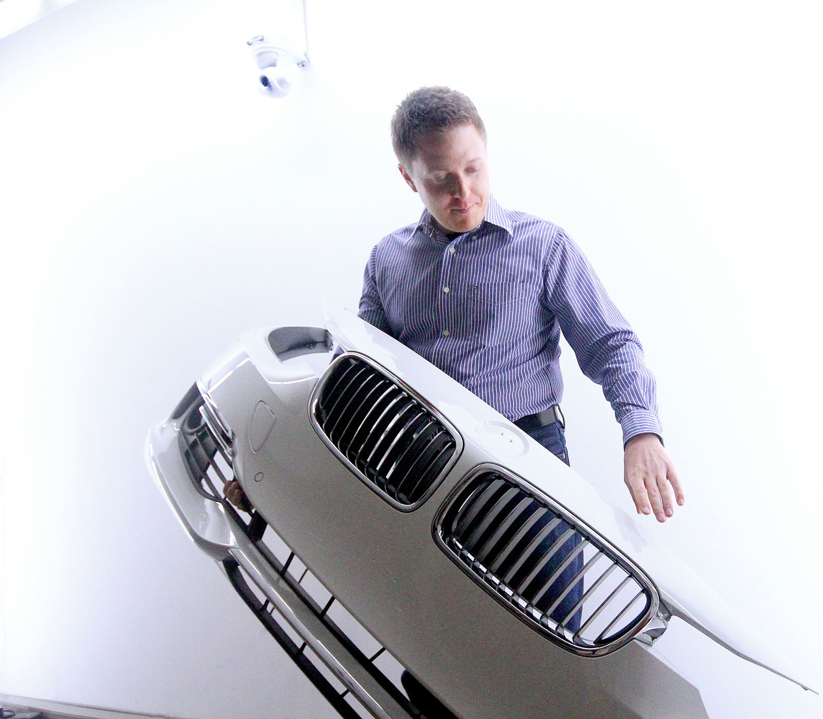 |
| A point of the finger is all it takes to send the defect in the paint to the QS inspection system, store it and document it. © Fraunhofer IOSB |
For production operations, quality assurance over the process chain is indispensable: it is the only way to detect problems at an early stage and lower additional costs. Fraunhofer researchers developed an efficient type of quality control: With a pointing gesture, employees can input any detected defects to car body parts into the inspection system, and document them there. The non-contact gesture-detection process will be on display at the 2013 Hannover Messe from 8 to 12 April.
With utter meticulousness, the quality control inspector examines a car bumper for defects in the paint work – ultimately, only impeccable body parts get sent to final assembly. If he finds a defect in the paint, just a point of the finger is all it takes to send the defect to the QS inspection system, store it and document it. The employee obtains visual feedback through a monitor that displays a 3D reconstruction of the bumper. At first glance, it might seem completely futuristic, though soon enough, it could become an everyday part of quality assurance: Researchers at the Fraunhofer Institute for Optronics, System Technologies and Image Exploitation IOSB in Karlsruhe engineered the intelligent gesture control system on behalf of the BMW Group. In the future, it should supersede today’s time-consuming test procedures. “Previously, the inspector had to note all defects that were detected, leave his workstation, go to the PC terminal, operate multiple input screens and then label the position of the defect and the defect type. That approach is laborious, time-intensive and prone to error,” asserts Alexander Schick, scientist at IOSB. The gesture control system, by contrast, improves the inspector’s working conditions considerably, and triggering substantial time savings – the employee can remain at his workstation and interact directly with the test object. “If the bumper is fine, then he swipes over it from left to right. In the event of damage, he points to the location of the defect,” says Schick.
3D tracking records people and objects in real time
This non-contact gesture-detection system is based on 3D data. Hence, the entire workstation must first be reconstructed in 3D. That includes the individual as well as the object with which he is working. “What does the inspector look like? Where is he situated? How does he move? What is he doing? Where is the object? – all of these data are required so that the pointing gesture can properly link to the bumper,” ex-
plains the researcher. In order to enable gesture control, the experts apply 3D-body tracking, which records the individual’s posture in real time. Even the car body parts are “tracked.” When it comes to this, the hardware requirements are minimal: A standard PC and two Microsoft Kinect systems – consisting of camera and 3D sensors – suffice in order to realize the reconstruction. Schick and his team developed the corresponding algorithms, which fuse multiple 2D and 3D images together, specifically for this kind of application, and adapted them to the standards of the BMW Group.
“The breeding ground for this technology is our Smart Control Room, where people can interact with the room quite naturally. They can use pointing gestures to operate remote displays – without any additional equipment. The room recognizes what actions are taking place at that moment, and offers the appropriate information and tools. Since gesture detection does not depend on display screens, this means we can im-
plement applications that use no monitors, like the gesture interaction here with real objects,” explains Schick. “It makes no difference what kind of object we are dealing with. Instead of a bumper, we could also track a different part.”
The technology can be subsequently integrated into existing production systems at little expense. Scientists could incorporate their effective process into the BMW Group’s system through a specialized interface module. The gesture detection system will be presented at the 2013 Hannover Messe, from 8 to 12 April, at the Fraunhofer joint exhibition booth in Hall 2, Booth D18.
Plans call for the installation of a prototype model at the BMW plant in Landshut in January 2013. Working in cooperation with quality control inspectors, the system will be fine-tuned onsite before it gets deployed to production in the future.
Source: Fraunhofer-Gesellschaft
Wednesday, 16 January 2013
Engineer making rechargeable batteries with layered nanomaterials
Engineerblogger
Jan 16, 2013
A Kansas State University researcher is developing more efficient ways to save costs, time and energy when creating nanomaterials and lithium-ion batteries.
Gurpreet Singh, assistant professor of mechanical and nuclear engineering, and his research team have published two recent articles on newer, cheaper and faster methods for creating nanomaterials that can be used for lithium-ion batteries. In the past year, Singh has published eight articles -- five of which involve lithium-ion battery research.
"We are exploring new methods for quick and cost-effective synthesis of two-dimensional materials for rechargeable battery applications," Singh said. "We are interested in this research because understanding lithium interaction with single-, double- and multiple-layer-thick materials will eventually allow us to design battery electrodes for practical applications. This includes batteries that show improved capacity, efficiency and longer life."
For the latest research, Singh's team created graphene films that are between two and 10 layers thick. Graphene is an atom-thick sheet of carbon. The researchers grew the graphene films on copper and nickel foils by quickly heating them in a furnace in the presence of controlled amounts of argon, hydrogen and methane gases. The team has been able to create these films in less than 30 minutes. Their work appears in the January issue of ACS-Applied Materials and Interfaces in an article titled "Synthesis of graphene films by rapid heating and quenching at ambient pressures and their electrochemical characterization."
The research is significant because the researchers created these graphene sheets by quickly heating and cooling the copper and nickel substrates at atmospheric pressures, meaning that scientists no longer need a vacuum to create few-layer-thick graphene films and can save energy, time and cost, Singh said.
The researchers used these graphene films to create the negative electrode of a lithium-ion cell and then studied the charge and discharge characteristics of this rechargeable battery. They found the graphene films grown on copper did not cycle the lithium ions and the battery capacity was negligible. But graphene grown on nickel showed improved performance because it was able to store and release lithium ions more efficiently.
"We believe that this behavior occurs because sheets of graphene on nickel are relatively thick near the grain boundaries and stacked in a well-defined manner -- called Bernal Stacking -- which provides multiple sites for easy uptake and release of lithium ions as the battery is discharged and charged," Singh said.
In a second research project, the researchers created tungsten disulfide nanosheets that were approximately 10 layers thick. Starting with bulk tungsten disulfide powder -- which is a type of dry lubricant used in the automotive industry -- the team was able to separate atomic layer thick sheets of tungsten disulfide in a strong acid solution. This simple method made it possible to produce sheets in large quantities. Much like graphene, tungsten disulfide also has a layered atomic structure, but the individual layers are three atoms thick.
The researchers found that these acid-treated tungsten disulfide sheets could also store and release lithium ions but in a different way. The lithium is stored through a conversion reaction in which tungsten disulfide dissociates to form tungsten and lithium sulfide as the cell is discharged. Unlike graphene, this reaction involves the transfer of at least two electrons per tungsten atom. This is important because researchers have long disregarded such compounds as battery anodes because of the difficulty associated with adding lithium to these materials, Singh said. It is only recently that the conversion reaction-based battery anodes have gained popularity.
"We also realize that tungsten disulfideis a heavy compound compared to state-of-the-art graphite used in current lithium-ion batteries," Singh said. "Therefore tungsten disulfide may not be an ideal electrode material for portable batteries."
The research appeared in a recent issue of the Journal of Physical Chemistry Letters in an article titled "Synthesis of surface-functionalized WS2 nanosheets and performance as Li-ion battery anodes."
Both projects are important because they can help scientists create nanomaterials in a cost-effective way. While many studies have focused on making graphene using low-pressure chemical processes, little research has been tried using rapid heating and cooling at atmospheric pressures, Singh said. Similarly, large quantities of single-layer and multiple-layer thick sheets of tungsten disulfide are needed for other applications.
"Interestingly, for most applications that involve this kind of battery research and corrosion prevention, films that are a few atoms thick are usually sufficient," Singh said. "Very high quality large area single-atom-thick films are not a necessity."
Other Kansas State University researchers involved in the projects include Romil Bhandavat and Lamuel David, both doctoral students in mechanical engineering, India, and Saksham Pahwa, a visiting undergraduate student, India. The graphene research involved University of Michigan researchers, including Zhaohui Zhong, assistant professor of electrical engineering and computer science, andGirish Kulkarni, doctoral candidate in electrical engineering.
Singh's work has been supported by the National Institute of Standards and Technology and the Kansas National Science Foundation Experimental Program to Stimulate Competitive Research program.
Singh plans future research to study how these layered nanomaterials can create better electrodes in the form of heterostructures, which are essentially three-dimensional stacked structures involving alternating layers of graphene and tungsten or molybdenum disulfide.
Source: Kansas State University
Additional Information:
Jan 16, 2013
 |
| We study the process of graphene growth on Cu and Ni substrates subjected to rapid heating (approximately 8 °C/s) and cooling cycles (approximately 10 °C/s) in a modified atmospheric pressure chemical vapor deposition furnace. Electron microscopy followed by Raman spectroscopy demonstrated successful synthesis of large-area few-layer graphene (FLG) films on both Cu and Ni substrates. The overall synthesis time was less than 30 min. Further, the as-synthesized films were directly utilized as anode material and their electrochemical behavior was studied in a lithium half-cell configuration. FLG on Cu (Cu-G) showed reduced lithium-intercalation capacity when compared with SLG, BLG and Bare-Cu suggesting its substrate protective nature (barrier to Li-ions). Although graphene films on Ni (Ni-G) showed better Li-cycling ability similar to that of other carbons suggesting that the presence of graphene edge planes (typical of Ni-G) is important in effective uptake and release of Li-ions in these materials. Source: ACS |
A Kansas State University researcher is developing more efficient ways to save costs, time and energy when creating nanomaterials and lithium-ion batteries.
Gurpreet Singh, assistant professor of mechanical and nuclear engineering, and his research team have published two recent articles on newer, cheaper and faster methods for creating nanomaterials that can be used for lithium-ion batteries. In the past year, Singh has published eight articles -- five of which involve lithium-ion battery research.
"We are exploring new methods for quick and cost-effective synthesis of two-dimensional materials for rechargeable battery applications," Singh said. "We are interested in this research because understanding lithium interaction with single-, double- and multiple-layer-thick materials will eventually allow us to design battery electrodes for practical applications. This includes batteries that show improved capacity, efficiency and longer life."
For the latest research, Singh's team created graphene films that are between two and 10 layers thick. Graphene is an atom-thick sheet of carbon. The researchers grew the graphene films on copper and nickel foils by quickly heating them in a furnace in the presence of controlled amounts of argon, hydrogen and methane gases. The team has been able to create these films in less than 30 minutes. Their work appears in the January issue of ACS-Applied Materials and Interfaces in an article titled "Synthesis of graphene films by rapid heating and quenching at ambient pressures and their electrochemical characterization."
The research is significant because the researchers created these graphene sheets by quickly heating and cooling the copper and nickel substrates at atmospheric pressures, meaning that scientists no longer need a vacuum to create few-layer-thick graphene films and can save energy, time and cost, Singh said.
The researchers used these graphene films to create the negative electrode of a lithium-ion cell and then studied the charge and discharge characteristics of this rechargeable battery. They found the graphene films grown on copper did not cycle the lithium ions and the battery capacity was negligible. But graphene grown on nickel showed improved performance because it was able to store and release lithium ions more efficiently.
"We believe that this behavior occurs because sheets of graphene on nickel are relatively thick near the grain boundaries and stacked in a well-defined manner -- called Bernal Stacking -- which provides multiple sites for easy uptake and release of lithium ions as the battery is discharged and charged," Singh said.
In a second research project, the researchers created tungsten disulfide nanosheets that were approximately 10 layers thick. Starting with bulk tungsten disulfide powder -- which is a type of dry lubricant used in the automotive industry -- the team was able to separate atomic layer thick sheets of tungsten disulfide in a strong acid solution. This simple method made it possible to produce sheets in large quantities. Much like graphene, tungsten disulfide also has a layered atomic structure, but the individual layers are three atoms thick.
The researchers found that these acid-treated tungsten disulfide sheets could also store and release lithium ions but in a different way. The lithium is stored through a conversion reaction in which tungsten disulfide dissociates to form tungsten and lithium sulfide as the cell is discharged. Unlike graphene, this reaction involves the transfer of at least two electrons per tungsten atom. This is important because researchers have long disregarded such compounds as battery anodes because of the difficulty associated with adding lithium to these materials, Singh said. It is only recently that the conversion reaction-based battery anodes have gained popularity.
"We also realize that tungsten disulfideis a heavy compound compared to state-of-the-art graphite used in current lithium-ion batteries," Singh said. "Therefore tungsten disulfide may not be an ideal electrode material for portable batteries."
The research appeared in a recent issue of the Journal of Physical Chemistry Letters in an article titled "Synthesis of surface-functionalized WS2 nanosheets and performance as Li-ion battery anodes."
Both projects are important because they can help scientists create nanomaterials in a cost-effective way. While many studies have focused on making graphene using low-pressure chemical processes, little research has been tried using rapid heating and cooling at atmospheric pressures, Singh said. Similarly, large quantities of single-layer and multiple-layer thick sheets of tungsten disulfide are needed for other applications.
"Interestingly, for most applications that involve this kind of battery research and corrosion prevention, films that are a few atoms thick are usually sufficient," Singh said. "Very high quality large area single-atom-thick films are not a necessity."
Other Kansas State University researchers involved in the projects include Romil Bhandavat and Lamuel David, both doctoral students in mechanical engineering, India, and Saksham Pahwa, a visiting undergraduate student, India. The graphene research involved University of Michigan researchers, including Zhaohui Zhong, assistant professor of electrical engineering and computer science, andGirish Kulkarni, doctoral candidate in electrical engineering.
Singh's work has been supported by the National Institute of Standards and Technology and the Kansas National Science Foundation Experimental Program to Stimulate Competitive Research program.
Singh plans future research to study how these layered nanomaterials can create better electrodes in the form of heterostructures, which are essentially three-dimensional stacked structures involving alternating layers of graphene and tungsten or molybdenum disulfide.
Source: Kansas State University
Additional Information:
Saturday, 12 January 2013
Good vibrations: Scientists recently developed a new microvibration excitation device
Engineerblogger
Jan 12, 2013
NPL scientists recently developed a new microvibration excitation device, which is currently under test at the European Space Agency (ESA) space test centre at ESTEC in Noordwijk, Holland.
The 'little shaker' device was produced as part of a technology research project for ESA to develop a prototype universal reference excitation unit which can be used to validate the performance of all kind of microvibration test facilities, traceable to ISO17025 levels of confidence and which can be deployed to perform inter facility comparison measurements.
The device is about the size of a shoe-box and generates small forces and torques (µN/µNm to single digit N/Nm range) at relatively low frequency (0.05 Hz to 10 Hz) in a controlled manner via reaction force against a moving mass. It can create force and torque along or about a single axis, and be repositioned in any orientation, to allow six-degree-of-freedom forces to be generated. The device is unique because there are currently no comparable means of producing highly repeatable forces and torques of this low magnitude in such a small, compact and portable mechanism.
Testing at the ESTEC space test center involved placing the device on Reaction Wheel Characterization Facility platform, activating it to create sinusoidal forces and moments in various orientations, and comparing the generated forces with those measured by the ESTEC facility.
Preliminary results are excellent and ESA now has a prototype device it can take to other facilities that will produce an identical drive signal, to allow comparisons of measurement results between facilities.
NPL was a natural partner for ESA on this project due to previous successful collaborations with challenging micro-thrust measurements. Additionally, NPL's role as the UK's National Measurement Institute provides confidence and experience in measurements traceable to primary standards and will be critical in allowing ESA to accredit their microvibration facility to the ISO 17025 standard in the future.
Source: NPL
Additional Information:
Jan 12, 2013
NPL scientists recently developed a new microvibration excitation device, which is currently under test at the European Space Agency (ESA) space test centre at ESTEC in Noordwijk, Holland.
 |
| The NPL excitation unit mounted on the ESA Reaction Wheel Characterization Facility |
The 'little shaker' device was produced as part of a technology research project for ESA to develop a prototype universal reference excitation unit which can be used to validate the performance of all kind of microvibration test facilities, traceable to ISO17025 levels of confidence and which can be deployed to perform inter facility comparison measurements.
The device is about the size of a shoe-box and generates small forces and torques (µN/µNm to single digit N/Nm range) at relatively low frequency (0.05 Hz to 10 Hz) in a controlled manner via reaction force against a moving mass. It can create force and torque along or about a single axis, and be repositioned in any orientation, to allow six-degree-of-freedom forces to be generated. The device is unique because there are currently no comparable means of producing highly repeatable forces and torques of this low magnitude in such a small, compact and portable mechanism.
Testing at the ESTEC space test center involved placing the device on Reaction Wheel Characterization Facility platform, activating it to create sinusoidal forces and moments in various orientations, and comparing the generated forces with those measured by the ESTEC facility.
Preliminary results are excellent and ESA now has a prototype device it can take to other facilities that will produce an identical drive signal, to allow comparisons of measurement results between facilities.
NPL was a natural partner for ESA on this project due to previous successful collaborations with challenging micro-thrust measurements. Additionally, NPL's role as the UK's National Measurement Institute provides confidence and experience in measurements traceable to primary standards and will be critical in allowing ESA to accredit their microvibration facility to the ISO 17025 standard in the future.
Source: NPL
Additional Information:
- Find out more about NPL's Dimensional research
Monday, 7 January 2013
Ford 1.0-Liter EcoBoost Engine Sets the Standard for Smoothness and Quietness in Small Engines
Engineerblogger
Jan 7, 2013
Start up Ford’s patented new 1.0-liter three-cylinder EcoBoost® engine and chances are you’ll have to look at the tachometer to verify that the engine is running.
Ford engineers always knew they could build a powerful, fuel-efficient three-cylinder engine. The real engineering magic would be solving the problem that has often sunk previous three-cylinder automobile engines – conquering the unpleasant vibrations that come from having an odd number of cylinders under the hood.
For Ford’s new three-cylinder engine to be successful, it would have to be a no-compromise engine. It could not force customers to choose between performance versus economy or responsiveness versus smoothness. It had to deliver it all and it had to be affordable.
The traditional way of reducing shaking forces in small-displacement engines is to install a counter-rotating balance shaft inside the motor that cancels out most vibrations. But the problem with a balance shaft, explains Andy Delicata, Ford of Europe manager of Powertrain Noise, Vibration and Harshness, is that it is heavy, expensive, and it reduces fuel economy.
The 1.0-liter’s NVH engineering team, led by Delicata at Ford Technical Centres in Dunton and Dagenham, England, attacked the problem by focusing on two areas – the engine’s front pulley and rear flywheel, and the mounting system that connects the powertrain with the car’s body.
The pulley and flywheel are unbalanced with weights that are placed precisely to counteract the natural shaking forces of the engine and drive the energy in a less sensitive direction. The engine mounts are designed to decouple as well as absorb the engine’s shaking forces, Delicata explained.
The result is one of the smoothest and quietest engines in Ford’s global lineup. “We like to compare the refinement of the 1.0-liter EcoBoost engine with what you would typically experience in a vehicle two or three classes up from Fiesta and Focus,” said Delicata.
The smoothness of the engine is complemented by class-leading quietness. Engineers in Dunton and Dagenham attacked engine noise at its many sources.
For instance, a super-compact, highly stiff cast-iron block structure and an integrated engine mounting bracket are crucial in absorbing noise energy. In addition to immersing the engine’s toothed rubber timing belts in oil, isolated fuel injectors electronically controlled for soft landing and a foam-covered engine collectively help keep noise and vibration from reaching the driver.
The 1.0-liter EcoBoost engine is off to a fast start in Europe. Since its launch in March in the Focus, the 1.0-liter EcoBoost engine has won four major international awards. In the Focus, the 1.0-liter engine accounts for about 30 percent of sales, no small feat in a part of the world where the diesel engine is king.
The 1.0-liter is just now launching in B-MAX and C-MAX, and will be available in North America next year in the redesigned 2014 Ford Fiesta.
Source: Ford Motor Company
Additional Information:
Jan 7, 2013
 |
| Ford CEO Alan Mulally kissing 1.0-liter EcoBoost engine |
- Innovative engine mounts, flywheel and pulley in the new 1.0-liter Ford EcoBoost® engine combine to dramatically reduce the vibrations that are inherent in three-cylinder engines
- Super-stiff block, isolated fuel injectors and oil-immersed timing belts help make 1.0-liter EcoBoost engine one of Ford’s quietest engines
- 1.0-liter EcoBoost engine debuts in North America in the redesigned 2014 Ford Fiesta
Start up Ford’s patented new 1.0-liter three-cylinder EcoBoost® engine and chances are you’ll have to look at the tachometer to verify that the engine is running.
Ford engineers always knew they could build a powerful, fuel-efficient three-cylinder engine. The real engineering magic would be solving the problem that has often sunk previous three-cylinder automobile engines – conquering the unpleasant vibrations that come from having an odd number of cylinders under the hood.
For Ford’s new three-cylinder engine to be successful, it would have to be a no-compromise engine. It could not force customers to choose between performance versus economy or responsiveness versus smoothness. It had to deliver it all and it had to be affordable.
The traditional way of reducing shaking forces in small-displacement engines is to install a counter-rotating balance shaft inside the motor that cancels out most vibrations. But the problem with a balance shaft, explains Andy Delicata, Ford of Europe manager of Powertrain Noise, Vibration and Harshness, is that it is heavy, expensive, and it reduces fuel economy.
The 1.0-liter’s NVH engineering team, led by Delicata at Ford Technical Centres in Dunton and Dagenham, England, attacked the problem by focusing on two areas – the engine’s front pulley and rear flywheel, and the mounting system that connects the powertrain with the car’s body.
The pulley and flywheel are unbalanced with weights that are placed precisely to counteract the natural shaking forces of the engine and drive the energy in a less sensitive direction. The engine mounts are designed to decouple as well as absorb the engine’s shaking forces, Delicata explained.
The result is one of the smoothest and quietest engines in Ford’s global lineup. “We like to compare the refinement of the 1.0-liter EcoBoost engine with what you would typically experience in a vehicle two or three classes up from Fiesta and Focus,” said Delicata.
The smoothness of the engine is complemented by class-leading quietness. Engineers in Dunton and Dagenham attacked engine noise at its many sources.
For instance, a super-compact, highly stiff cast-iron block structure and an integrated engine mounting bracket are crucial in absorbing noise energy. In addition to immersing the engine’s toothed rubber timing belts in oil, isolated fuel injectors electronically controlled for soft landing and a foam-covered engine collectively help keep noise and vibration from reaching the driver.
The 1.0-liter EcoBoost engine is off to a fast start in Europe. Since its launch in March in the Focus, the 1.0-liter EcoBoost engine has won four major international awards. In the Focus, the 1.0-liter engine accounts for about 30 percent of sales, no small feat in a part of the world where the diesel engine is king.
The 1.0-liter is just now launching in B-MAX and C-MAX, and will be available in North America next year in the redesigned 2014 Ford Fiesta.
Source: Ford Motor Company
Additional Information:
Saturday, 5 January 2013
How a computer game could radically alter manufacturing
Engineerblogger
Jan 4, 2013

Here at The Engineer we’re used to explaining difficult concepts, whether it’s nuclear fusion or spintronics (actually I’m still not sure about that one). It helps that we have a receptive and enthusiastic audience and are tackling subject material that is usually instantly exciting.
But what if you had to explain something with less obvious appeal to people who think you might be wasting their time, for example, a complex new manufacturing business model to a group of sceptical bean counters? It’s probably not a conversation you’d want to have at a dinner party.
The answer to this might be to make the explanation into a game, according to one research group at least. Make the process fun, entertaining and engaging, and the audience might be more likely to understand and remember the concept, and perhaps even become more enthusiastic about it.
A team led by Aston University Business School are about to do just this by starting a five-year research project on the gamification of explaining servitisation. Now comes the bit where I explain what this boring and complicated-sounding concept actually is.
A product service system (PSS) is a business model where a firm offers both products and services. Rolls-Royce, for example, is well known for earning around 50 per cent of its revenue through service and support contracts, providing things such as maintenance and advice to customers that also buy its goods. Simply put, servitisation is when a straightforward manufacturing company adopts this model.
Particularly in developed marketplaces and economies, servitisation offers companies a chance to make more money than they would simply by selling products and competing against other manufacturers. Described like this, it sounds rather simple and very attractive. But making it a reality is a far more complex procedure with many barriers, and so servitisation of manufacturing firms has been slow.
Prof Tim Baines of Aston University argues that one of the biggest barriers to adoption of PSS is just explaining how the process of servitisation works. ‘To try to get those ideas across to someone in a manufacturing company in five or 10 minutes in a way that makes sense to them is quite challenging,’ he says.
This is where he believes gamification could come in. This is another slightly off-putting piece of jargon that basically means turning a process into a game. It’s not a new concept but has found growing popularity in recent years thanks to the growth of the internet and smartphones. There are any number of websites and apps that encourage you to do something by making it a game and rewarding you in some for participation.
For example, if you want to get fit but struggle to find the motivation, an app on your phone can monitor your progress to give you encouragement, telling you how many calories you’ve burnt or giving you badges for completing certain levels. One app even asks you to image you’re being chased by zombies and the only way to escape them is to run to a certain place.
But how will this work for explaining servitisation? Baines is planning to work with the Serious Games Institute at Coventry University and Sheffield’s Advanced Manufacturing Research Centre to create a computer simulation of a business adopting PSS. Companies, including Ford and Xerox, will then be brought in to test the game. ‘One of the big barriers is understanding, getting across the basic ideas and the language used, an appreciation of what it can actually mean,’ says Baines.
‘We’ll create a demonstration first of all so that we can communicate to the gaming community what we’re trying to do. The big hurdle is translating between these two communities, explaining to the gaming community what it is that we’re trying to model and them explaining to us what makes an engaging game. We’ve got to try to find the middle ground and from that we’ll create the basics of the game.’
It would be easy to write this concept of gamification off as a fad or a buzzword. For one thing, it doesn’t sound like the most fun idea for a game but, then again, there have been whole series of popular computer games designed around simulating real-life industries (Sim City, for example). And this won’t be the first time games are used to explain manufacturing concepts. Team games have been used before to demonstrate and introduce Western manufacturers to the Japanese-originated ideas of lean manufacturing.
Perhaps it will take more than a computer game to persuade companies to adopt dramatically different business models, but Baines hopes the game will do more than just change individual’s minds. ‘I would like it to be something quite pervasive that people inside the organisation become aware of and have a go at it, and for the top managers to hear about it not just from academics but also from people within the organisation who get to know about this thing called servitisation from playing the game.’
The game will also serve as a way for academics to further study servitisation so they can better understand the barriers to adopting PSS when it is attempted by real companies.
With gamification spreading even into business management techniques, it’s interesting to consider how else it could be used in manufacturing or other parts of the economy. Perhaps games could become a more common sight at work, motivating people to complete tasks or reach certain levels of achievement. On the other hand, you could argue we already run such a reward system. It’s called getting paid.
Source: The Engineer
Jan 4, 2013

Here at The Engineer we’re used to explaining difficult concepts, whether it’s nuclear fusion or spintronics (actually I’m still not sure about that one). It helps that we have a receptive and enthusiastic audience and are tackling subject material that is usually instantly exciting.
But what if you had to explain something with less obvious appeal to people who think you might be wasting their time, for example, a complex new manufacturing business model to a group of sceptical bean counters? It’s probably not a conversation you’d want to have at a dinner party.
The answer to this might be to make the explanation into a game, according to one research group at least. Make the process fun, entertaining and engaging, and the audience might be more likely to understand and remember the concept, and perhaps even become more enthusiastic about it.
A team led by Aston University Business School are about to do just this by starting a five-year research project on the gamification of explaining servitisation. Now comes the bit where I explain what this boring and complicated-sounding concept actually is.
A product service system (PSS) is a business model where a firm offers both products and services. Rolls-Royce, for example, is well known for earning around 50 per cent of its revenue through service and support contracts, providing things such as maintenance and advice to customers that also buy its goods. Simply put, servitisation is when a straightforward manufacturing company adopts this model.
Particularly in developed marketplaces and economies, servitisation offers companies a chance to make more money than they would simply by selling products and competing against other manufacturers. Described like this, it sounds rather simple and very attractive. But making it a reality is a far more complex procedure with many barriers, and so servitisation of manufacturing firms has been slow.
Prof Tim Baines of Aston University argues that one of the biggest barriers to adoption of PSS is just explaining how the process of servitisation works. ‘To try to get those ideas across to someone in a manufacturing company in five or 10 minutes in a way that makes sense to them is quite challenging,’ he says.
This is where he believes gamification could come in. This is another slightly off-putting piece of jargon that basically means turning a process into a game. It’s not a new concept but has found growing popularity in recent years thanks to the growth of the internet and smartphones. There are any number of websites and apps that encourage you to do something by making it a game and rewarding you in some for participation.
For example, if you want to get fit but struggle to find the motivation, an app on your phone can monitor your progress to give you encouragement, telling you how many calories you’ve burnt or giving you badges for completing certain levels. One app even asks you to image you’re being chased by zombies and the only way to escape them is to run to a certain place.
But how will this work for explaining servitisation? Baines is planning to work with the Serious Games Institute at Coventry University and Sheffield’s Advanced Manufacturing Research Centre to create a computer simulation of a business adopting PSS. Companies, including Ford and Xerox, will then be brought in to test the game. ‘One of the big barriers is understanding, getting across the basic ideas and the language used, an appreciation of what it can actually mean,’ says Baines.
‘We’ll create a demonstration first of all so that we can communicate to the gaming community what we’re trying to do. The big hurdle is translating between these two communities, explaining to the gaming community what it is that we’re trying to model and them explaining to us what makes an engaging game. We’ve got to try to find the middle ground and from that we’ll create the basics of the game.’
It would be easy to write this concept of gamification off as a fad or a buzzword. For one thing, it doesn’t sound like the most fun idea for a game but, then again, there have been whole series of popular computer games designed around simulating real-life industries (Sim City, for example). And this won’t be the first time games are used to explain manufacturing concepts. Team games have been used before to demonstrate and introduce Western manufacturers to the Japanese-originated ideas of lean manufacturing.
Perhaps it will take more than a computer game to persuade companies to adopt dramatically different business models, but Baines hopes the game will do more than just change individual’s minds. ‘I would like it to be something quite pervasive that people inside the organisation become aware of and have a go at it, and for the top managers to hear about it not just from academics but also from people within the organisation who get to know about this thing called servitisation from playing the game.’
The game will also serve as a way for academics to further study servitisation so they can better understand the barriers to adopting PSS when it is attempted by real companies.
With gamification spreading even into business management techniques, it’s interesting to consider how else it could be used in manufacturing or other parts of the economy. Perhaps games could become a more common sight at work, motivating people to complete tasks or reach certain levels of achievement. On the other hand, you could argue we already run such a reward system. It’s called getting paid.
Source: The Engineer
New 2D material for next generation high-speed electronics
Engineerblogger
Jan 4, 2013
Scientists at CSIRO and RMIT University have produced a new two-dimensional material that could revolutionise the electronics market, making “nano” more than just a marketing term.
The material – made up of layers of crystal known as molybdenum oxides – has unique properties that encourage the free flow of electrons at ultra-high speeds.
In a paper published in the January issue of materials science journal Advanced Materials, the researchers explain how they adapted a revolutionary material known as graphene to create a new conductive nano-material.
Graphene was created in 2004 by scientists in the UK and won its inventors a Nobel Prize in 2010. While graphene supports high speed electrons, its physical properties prevent it from being used for high-speed electronics.
The CSIRO's Dr Serge Zhuiykov said the new nano-material was made up of layered sheets – similar to graphite layers that make up a pencil's core.
"Within these layers, electrons are able to zip through at high speeds with minimal scattering," Dr Zhuiykov said.
"The importance of our breakthrough is how quickly and fluently electrons – which conduct electricity – are able to flow through the new material."
RMIT's Professor Kourosh Kalantar-zadeh said the researchers were able to remove "road blocks" that could obstruct the electrons, an essential step for the development of high-speed electronics.
"Instead of scattering when they hit road blocks, as they would in conventional materials, they can simply pass through this new material and get through the structure faster," Professor Kalantar-zadeh said.
"Quite simply, if electrons can pass through a structure quicker, we can build devices that are smaller and transfer data at much higher speeds.
"While more work needs to be done before we can develop actual gadgets using this new 2D nano-material, this breakthrough lays the foundation for a new electronics revolution and we look forward to exploring its potential."
In the paper titled 'Enhanced Charge Carrier Mobility in Two-Dimensional High Dielectric Molybdenum Oxide,' the researchers describe how they used a process known as "exfoliation" to create layers of the material ~11nm thick.
The material was manipulated to convert it into a semiconductor and nanoscale transistors were then created using molybdenum oxide.
The result was electron mobility values of >1,100 cm2/Vs – exceeding the current industry standard for low dimensional silicon.
The work, with RMIT doctoral researcher Sivacarendran Balendhran as the lead author, was supported by the CSIRO Sensors and Sensor Networks Transformational Capability Platform and the CSIRO Materials Science and Engineering Division.
It was also a result of collaboration between researchers from Monash University, University of California – Los Angeles (UCLA), CSIRO, Massachusetts Institute of Technology (MIT) and RMIT.
Source: CSIRO
Jan 4, 2013
 |
| Artist impression of high carrier mobility through layered molybdenum oxide crystal lattice. Credit: Dr Daniel J White, ScienceFX |
Scientists at CSIRO and RMIT University have produced a new two-dimensional material that could revolutionise the electronics market, making “nano” more than just a marketing term.
The material – made up of layers of crystal known as molybdenum oxides – has unique properties that encourage the free flow of electrons at ultra-high speeds.
In a paper published in the January issue of materials science journal Advanced Materials, the researchers explain how they adapted a revolutionary material known as graphene to create a new conductive nano-material.
Graphene was created in 2004 by scientists in the UK and won its inventors a Nobel Prize in 2010. While graphene supports high speed electrons, its physical properties prevent it from being used for high-speed electronics.
The CSIRO's Dr Serge Zhuiykov said the new nano-material was made up of layered sheets – similar to graphite layers that make up a pencil's core.
"Within these layers, electrons are able to zip through at high speeds with minimal scattering," Dr Zhuiykov said.
"The importance of our breakthrough is how quickly and fluently electrons – which conduct electricity – are able to flow through the new material."
RMIT's Professor Kourosh Kalantar-zadeh said the researchers were able to remove "road blocks" that could obstruct the electrons, an essential step for the development of high-speed electronics.
"Instead of scattering when they hit road blocks, as they would in conventional materials, they can simply pass through this new material and get through the structure faster," Professor Kalantar-zadeh said.
"Quite simply, if electrons can pass through a structure quicker, we can build devices that are smaller and transfer data at much higher speeds.
"While more work needs to be done before we can develop actual gadgets using this new 2D nano-material, this breakthrough lays the foundation for a new electronics revolution and we look forward to exploring its potential."
In the paper titled 'Enhanced Charge Carrier Mobility in Two-Dimensional High Dielectric Molybdenum Oxide,' the researchers describe how they used a process known as "exfoliation" to create layers of the material ~11nm thick.
The material was manipulated to convert it into a semiconductor and nanoscale transistors were then created using molybdenum oxide.
The result was electron mobility values of >1,100 cm2/Vs – exceeding the current industry standard for low dimensional silicon.
The work, with RMIT doctoral researcher Sivacarendran Balendhran as the lead author, was supported by the CSIRO Sensors and Sensor Networks Transformational Capability Platform and the CSIRO Materials Science and Engineering Division.
It was also a result of collaboration between researchers from Monash University, University of California – Los Angeles (UCLA), CSIRO, Massachusetts Institute of Technology (MIT) and RMIT.
Source: CSIRO
Sunday, 9 September 2012
Honda Develops New Technology to Weld Together Steel and Aluminum and Achieves World's First Application to the Frame of a Mass-production Vehicle
Engineerblogger
Sept. 9, 2012
Honda Motor Company announced that it has newly developed a technology for the continuous welding of the dissimilar metals of steel and aluminum and applied it for the first time in the world to the subframe of a mass-production vehicle, a key component of a vehicle body frame. Honda will adopt this technology first to the North American version of the all-new 2013 Accord, which will go on sale in the United States on September 19, 2012, and will expand application sequentially to other models.
Striving to reduce vehicle weight in order to increase fuel economy, Honda focused on Friction Stir Welding (FSW) and developed a new technology for the continuous welding of steel and aluminum. This technology generates a new and stable metallic bonding between steel and aluminum by moving a rotating tool on the top of the aluminum which is lapped over the steel with high pressure. As a result, the welding strength becomes equal to or beyond conventional Metal Inert Gas (MIG) welding*1.
This new technology contributes to an improvement in fuel economy by reducing body weight by 25% compared to a conventional steel subframe. In addition, electricity consumption during the welding process is reduced by approximately 50%. It also enabled a change in the structure of the subframe and the mounting point of suspension, which increased the rigidity of the mounting point by 20% and also contributed to the vehicle’s dynamic performance.
Furthermore, Honda established a new method to apply this technology to mass-production vehicles. Conventionally, FSW required use of large equipment, but Honda developed a FSW continuous welding system applied to a highly versatile industrial robot. This system also can be used for aluminum-to-aluminum welding and thus, the welding system with the same specifications can be used for production of a full-aluminum subframe.
Honda also developed a non-destructive inspection system*2 using a highly-sensitive infrared camera and laser beam, which enables an in-line inspection of the bonding location for every unit.
*1 A welding technique most commonly used for welding of identical materials such as steel-to-steel or aluminum-to-aluminum
*2A system that evaluates quality without actually destructing the parts
Source: Honda
Sept. 9, 2012
 |
| Front Subframe |
Honda Motor Company announced that it has newly developed a technology for the continuous welding of the dissimilar metals of steel and aluminum and applied it for the first time in the world to the subframe of a mass-production vehicle, a key component of a vehicle body frame. Honda will adopt this technology first to the North American version of the all-new 2013 Accord, which will go on sale in the United States on September 19, 2012, and will expand application sequentially to other models.
 |
| Conceptual diagram of FSW of dissimilar metals |
Striving to reduce vehicle weight in order to increase fuel economy, Honda focused on Friction Stir Welding (FSW) and developed a new technology for the continuous welding of steel and aluminum. This technology generates a new and stable metallic bonding between steel and aluminum by moving a rotating tool on the top of the aluminum which is lapped over the steel with high pressure. As a result, the welding strength becomes equal to or beyond conventional Metal Inert Gas (MIG) welding*1.
This new technology contributes to an improvement in fuel economy by reducing body weight by 25% compared to a conventional steel subframe. In addition, electricity consumption during the welding process is reduced by approximately 50%. It also enabled a change in the structure of the subframe and the mounting point of suspension, which increased the rigidity of the mounting point by 20% and also contributed to the vehicle’s dynamic performance.
Furthermore, Honda established a new method to apply this technology to mass-production vehicles. Conventionally, FSW required use of large equipment, but Honda developed a FSW continuous welding system applied to a highly versatile industrial robot. This system also can be used for aluminum-to-aluminum welding and thus, the welding system with the same specifications can be used for production of a full-aluminum subframe.
Honda also developed a non-destructive inspection system*2 using a highly-sensitive infrared camera and laser beam, which enables an in-line inspection of the bonding location for every unit.
*1 A welding technique most commonly used for welding of identical materials such as steel-to-steel or aluminum-to-aluminum
*2A system that evaluates quality without actually destructing the parts
Source: Honda
Could ancient Egyptians hold the key to 3D printed ceramics?
Engineerblogger
Sept 3, 2012

Video: Professor Stephen Hoskins shares more about the latest 3D printing methods in ceramics in this insightful interview.
A 7,000 year old technique, known as Egyptian Paste (also known as Faience), could offer a potential process and material for use in the latest 3D printing techniques of ceramics, according to researchers at UWE Bristol.
Professor Stephen Hoskins, Director of UWE's Centre for Fine Print Research and David Huson, Research Fellow, have received funding from the Arts and Humanities Research Council (AHRC to undertake a major investigation into a self-glazing 3D printed ceramic, inspired by ancient Egyptian Faience ceramic techniques. The process they aim to develop would enable ceramic artists, designers and craftspeople to print 3D objects in a ceramic material which can be glazed and vitrified in one firing.
The researchers believe that it possible to create a contemporary 3D printable, once-fired, self-glazing, non-plastic ceramic material that exhibits the characteristics and quality of Egyptian Faience.
Faience was first used in the 5th Millennium BC and was the first glazed ceramic material invented by man. Faience was not made from clay (but instead composed of quartz and alkali fluxes) and is distinct from Italian Faience or Majolica, which is a tin, glazed earthenware. (The earliest Faience is invariably blue or green, exhibiting the full range of shades between them, and the colouring material was usually copper). It is the self-glazing properties of Faience that are of interest for this research project.
Current research in the field of 3D printing concentrates on creating functional materials to form physical models. The materials currently used in the 3D printing process, in which layers are added to build up a 3D form, are commonly: UV polymer resins, hot melted 'abs' plastic and inkjet binder or laser sintered, powder materials. These techniques have previously been known as rapid prototyping (RP). With the advent of better materials and equipment some RP of real materials is now possible. These processes are increasingly being referred to as solid 'free-form fabrication' (SFF) or additive layer manufacture. The UWE research team have focused previously on producing a functional, printable clay body.
This three-year research project will investigate three methods of glazing used by the ancient Egyptians: 'application glazing', similar to modern glazing methods; 'efflorescent glazing' which uses water-soluble salts; and 'cementation glazing', a technique where the object is buried in a glazing powder in a protective casing, then fired.These techniques will be used as a basis for developing contemporary printable alternatives
Professor Hoskins explains, “It is fascinating to think that some of these ancient processes, in fact the very first glazed ceramics every created by humans, could have relevance to the advanced printing technology of today. We hope to create a self-glazing 3D printed ceramic which only requires one firing from conception to completion rather than the usual two. This would be a radical step-forward in the development of 3D printing technologies. As part of the project we will undertake case studies of craft, design and fine art practitioners to contribute to the project, so that our work reflects the knowledge and understanding of artists and reflects the way in which artists work.”
The project includes funding for a three-year full-time PhD bursary to research a further method used by the Egyptians, investigating coloured 'frit', a substance used in glazing and enamels. This student will research this method, investigating the use of coloured frits and oxides to try and create as full a colour range as possible. Once developed, this body will be used to create a ceramic extrusion paste that can be printed with a low-cost 3D printer. A programme of work will be undertaken to determine the best rates of deposition, the inclusion of flocculants and methods of drying through heat whilst printing.
This project offers the theoretical possibility of a printed, single fired, glazed ceramic object - something that is impossible with current technology.
Source: University of the West of England
Sept 3, 2012
Video: Professor Stephen Hoskins shares more about the latest 3D printing methods in ceramics in this insightful interview.
A 7,000 year old technique, known as Egyptian Paste (also known as Faience), could offer a potential process and material for use in the latest 3D printing techniques of ceramics, according to researchers at UWE Bristol.
Professor Stephen Hoskins, Director of UWE's Centre for Fine Print Research and David Huson, Research Fellow, have received funding from the Arts and Humanities Research Council (AHRC to undertake a major investigation into a self-glazing 3D printed ceramic, inspired by ancient Egyptian Faience ceramic techniques. The process they aim to develop would enable ceramic artists, designers and craftspeople to print 3D objects in a ceramic material which can be glazed and vitrified in one firing.
The researchers believe that it possible to create a contemporary 3D printable, once-fired, self-glazing, non-plastic ceramic material that exhibits the characteristics and quality of Egyptian Faience.
Faience was first used in the 5th Millennium BC and was the first glazed ceramic material invented by man. Faience was not made from clay (but instead composed of quartz and alkali fluxes) and is distinct from Italian Faience or Majolica, which is a tin, glazed earthenware. (The earliest Faience is invariably blue or green, exhibiting the full range of shades between them, and the colouring material was usually copper). It is the self-glazing properties of Faience that are of interest for this research project.
Current research in the field of 3D printing concentrates on creating functional materials to form physical models. The materials currently used in the 3D printing process, in which layers are added to build up a 3D form, are commonly: UV polymer resins, hot melted 'abs' plastic and inkjet binder or laser sintered, powder materials. These techniques have previously been known as rapid prototyping (RP). With the advent of better materials and equipment some RP of real materials is now possible. These processes are increasingly being referred to as solid 'free-form fabrication' (SFF) or additive layer manufacture. The UWE research team have focused previously on producing a functional, printable clay body.
This three-year research project will investigate three methods of glazing used by the ancient Egyptians: 'application glazing', similar to modern glazing methods; 'efflorescent glazing' which uses water-soluble salts; and 'cementation glazing', a technique where the object is buried in a glazing powder in a protective casing, then fired.These techniques will be used as a basis for developing contemporary printable alternatives
Professor Hoskins explains, “It is fascinating to think that some of these ancient processes, in fact the very first glazed ceramics every created by humans, could have relevance to the advanced printing technology of today. We hope to create a self-glazing 3D printed ceramic which only requires one firing from conception to completion rather than the usual two. This would be a radical step-forward in the development of 3D printing technologies. As part of the project we will undertake case studies of craft, design and fine art practitioners to contribute to the project, so that our work reflects the knowledge and understanding of artists and reflects the way in which artists work.”
The project includes funding for a three-year full-time PhD bursary to research a further method used by the Egyptians, investigating coloured 'frit', a substance used in glazing and enamels. This student will research this method, investigating the use of coloured frits and oxides to try and create as full a colour range as possible. Once developed, this body will be used to create a ceramic extrusion paste that can be printed with a low-cost 3D printer. A programme of work will be undertaken to determine the best rates of deposition, the inclusion of flocculants and methods of drying through heat whilst printing.
This project offers the theoretical possibility of a printed, single fired, glazed ceramic object - something that is impossible with current technology.
Source: University of the West of England
Manufacturing crack-resistant lightweight components
Enginerblogger
Sept 9, 2012
Cars, roof structures and bridges should become increasingly lighter, with the same stability, and thus save energy and materials. New high-strength steel is superbly suited for the needed lightweight design, because it can also withstand extremely heavy stresses. Yet these materials also betray a disadvantage: with increasing strength their susceptibility to cold cracking rises when welded. These miniscule fractures might form as the welded joints cool off – typically at temperatures below 200°C. In a worst case scenario, the welding seams would crack. For this reason, many industrial sectors are reluctant to employ these promising high-strength steel.
Scientists at the Fraunhofer Institute for Mechanics of Materials IWM in Freiburg, in conjunction with the Chair of Joining and Welding Technology LFT at Brandenburg University of Technology Cottbus (BTU) developed a new process for making cold cracking more predictable. “We are able to compute the probability of cold cracking as early as the design stage of a component, and immediately run through corrective measures as well,” explains Frank Schweizer of the IWM. Because whether such cold cracking occurs, and how quickly, depends on how high the concentration of hydrogen in the steel is, how the residual stress turns out, and how its microstructure is configured. Predicting the probability of cracking has been difficult until now. Manufacturers used to conduct expensive testing, for example by applying an increasingly higher tensile stress to a sample component, and then analyse what stress level would cause cracking. Not only are these tests time-consuming and cost-intensive, the findings can-
not be applied to subsequent components on a one-to-one basis – because the geometry of the component has a decisive influence on crack formation. Even currently available computer simulations failed to deliver the desired predictive accuracy for real components.
Lowering production costs, shortening development phases
The new approach could markedly reduce such costly methods in the future – and thus lower production costs while shortening development phases. The experts at LFT set up a special test, in order to precisely determine the cracking criterion on samples of highstrength steel. Beside typical influencing factors like hydrogen content, residual stresses and material structures that can be adjusted in at the same time, they also take into account the temperature gradients that emerge in the welding process.
The experts at IWM feed a computer simulation with this criterion in order to analyze the threat of cold cracking in random components and geometries. “This way, we can locate the areas on a welding seam at risk of cold cracking, for each point and at any time in the simulated welding process,” explains Frank Schweizer. The researchers can also get a preliminary look at the effects of any countermeasures, and make the necessary adjustments. To do so, they transfert the results back into the simulation, in order to fine-tune them there.
In the future, with the aid of this process, manufacturers of vehicles and machines could be able to define non-critical welding parameters and limiting conditions for their materials in advance – and thus establish a substantially more efficient and safer production process. This is especially relevant to materials that are difficult to weld, with very narrow processing windows regarding welding parameters or the pre- and post-heating temperatures. Fraunhofer IWM and LFT, in cooperation with Robert Bosch GmbH and ThyssenKrupp Steel Europe AG, are currently testing their new process on laser beam-welded demonstration models made of high-strength steels.
Sept 9, 2012
 |
| In this test, the material sample is heated to welding temperature to determine its critical conditions for the formation of cold cracking. © Chair of Joining and Welding Technology at the Brandenburg University of Technology |
Scientists at the Fraunhofer Institute for Mechanics of Materials IWM in Freiburg, in conjunction with the Chair of Joining and Welding Technology LFT at Brandenburg University of Technology Cottbus (BTU) developed a new process for making cold cracking more predictable. “We are able to compute the probability of cold cracking as early as the design stage of a component, and immediately run through corrective measures as well,” explains Frank Schweizer of the IWM. Because whether such cold cracking occurs, and how quickly, depends on how high the concentration of hydrogen in the steel is, how the residual stress turns out, and how its microstructure is configured. Predicting the probability of cracking has been difficult until now. Manufacturers used to conduct expensive testing, for example by applying an increasingly higher tensile stress to a sample component, and then analyse what stress level would cause cracking. Not only are these tests time-consuming and cost-intensive, the findings can-
not be applied to subsequent components on a one-to-one basis – because the geometry of the component has a decisive influence on crack formation. Even currently available computer simulations failed to deliver the desired predictive accuracy for real components.
Lowering production costs, shortening development phases
The new approach could markedly reduce such costly methods in the future – and thus lower production costs while shortening development phases. The experts at LFT set up a special test, in order to precisely determine the cracking criterion on samples of highstrength steel. Beside typical influencing factors like hydrogen content, residual stresses and material structures that can be adjusted in at the same time, they also take into account the temperature gradients that emerge in the welding process.
The experts at IWM feed a computer simulation with this criterion in order to analyze the threat of cold cracking in random components and geometries. “This way, we can locate the areas on a welding seam at risk of cold cracking, for each point and at any time in the simulated welding process,” explains Frank Schweizer. The researchers can also get a preliminary look at the effects of any countermeasures, and make the necessary adjustments. To do so, they transfert the results back into the simulation, in order to fine-tune them there.
In the future, with the aid of this process, manufacturers of vehicles and machines could be able to define non-critical welding parameters and limiting conditions for their materials in advance – and thus establish a substantially more efficient and safer production process. This is especially relevant to materials that are difficult to weld, with very narrow processing windows regarding welding parameters or the pre- and post-heating temperatures. Fraunhofer IWM and LFT, in cooperation with Robert Bosch GmbH and ThyssenKrupp Steel Europe AG, are currently testing their new process on laser beam-welded demonstration models made of high-strength steels.
Boaz Almog “levitates” a superconductor
Engineerblogger
Sept 9, 2012
How can a super-thin 3-inch disk levitate something 70,000 times its own weight? In a riveting demonstration, Boaz Almog shows how a phenomenon known as quantum locking allows a superconductor disk to float over a magnetic rail -- completely frictionlessly and with zero energy loss.
Experiment: Prof. Guy Deutscher, Mishael Azoulay, Boaz Almog, of the High Tc Superconductivity Group, School of Physics and Astronomy, Tel Aviv University.
Source: TED
Sept 9, 2012
How can a super-thin 3-inch disk levitate something 70,000 times its own weight? In a riveting demonstration, Boaz Almog shows how a phenomenon known as quantum locking allows a superconductor disk to float over a magnetic rail -- completely frictionlessly and with zero energy loss.
Experiment: Prof. Guy Deutscher, Mishael Azoulay, Boaz Almog, of the High Tc Superconductivity Group, School of Physics and Astronomy, Tel Aviv University.
Source: TED
Saturday, 8 September 2012
Researchers create tiny, wirelessly powered cardiac device
Engineerblogger
Sept 9, 2012
Stanford electrical engineers overturn existing models to demonstrate the feasibility of a millimeter-sized, wirelessly powered cardiac device. The findings, say the researchers, could dramatically alter the scale of medical devices implanted in the human body.
A team of engineers at Stanford has demonstrated the feasibility of a super-small, implantable cardiac device that gets its power not from batteries but from radio waves transmitted from a small power device on the surface of the body.
The implanted device is contained in a cube just 0.8 millimeter on a side. It could fit on the head of pin.
The findings were published in the journal Applied Physics Letters. In their paper, the researchers demonstrated wireless power transfer to a millimeter-sized device implanted 5 centimeters inside the chest on the surface of the heart – a depth once thought out of reach for wireless power transmission.
The engineers say the research is a major step toward a day when all implants are driven wirelessly. Beyond the heart, they believe such devices might include swallowable endoscopes – so-called "pillcams" that travel the digestive tract – permanent pacemakers and precision brain stimulators – virtually any medical applications where device size and power matter.
A revolution in the body
Implantable medical devices in the human body have revolutionized medicine. Hundreds of thousands if not millions of pacemakers, cochlear implants and drug pumps are today helping patients live relatively normal lives, but these devices are not without engineering challenges.
First, they require power, which means batteries, and batteries are bulky. In a device like a pacemaker, the battery alone accounts for as much as half the volume of the device. Second, batteries have finite lives. New surgery is needed when they wane.
"Wireless power solves both challenges," said Ada Poon, assistant professor of electrical engineering, who headed up the research. She was assisted by Sanghoek Kim and John Ho, both doctoral candidates in her lab.
Last year, Poon made headlines when she demonstrated a wirelessly powered, self-propelled device capable of swimming through the bloodstream. To get there she needed to overturn some long-held assumptions about delivery of wireless power through the human body.
Her latest device works by a combination of inductive and radiative transmission of power. Both are types of electromagnetic transfer in which a transmitter sends radio waves to a coil of wire inside the body. The radio waves produce an electrical current in the coil sufficient to operate a small device.
There is an indirect relationship between the frequency of the transmitted radio waves and the size of the receiving antenna. That is, to deliver a desired level of power, lower frequency waves require bigger coils. Higher frequency waves can work with smaller coils.
"For implantable medical devices, therefore, the goal is a high-frequency transmitter and a small receiver, but there is one big hurdle," Kim said.
Ignoring consensus
Existing mathematical models have held that high-frequency radio waves do not penetrate far enough into human tissue, necessitating the use of low-frequency transmitters and large antennas – too large to be practical for implantable devices.
Ignoring the consensus, Poon proved the models wrong. Human tissues dissipate electric fields quickly, it is true, but radio waves can travel in a different way – as alternating waves of electric and magnetic fields. With the correct equations in hand, she discovered that high-frequency signals travel much deeper than anyone suspected.
"In fact, to achieve greater power efficiency, it is actually advantageous that human tissue is a very poor electrical conductor," said Kim. "If it were a good conductor, it would absorb energy, create heating and prevent sufficient power from reaching the implant."
According to their revised models, the researchers found that the maximum power transfer through human tissue occurs at about 1.7 billion cycles per second, much higher than previously thought.
"In this high-frequency range, we can increase power transfer by about 10 times over earlier devices," said Ho, who honed the mathematical models.
The discovery meant that the team could shrink the receiving antenna by a factor of 10 as well, to a scale that makes wireless implantable devices feasible. At the optimal frequency, a millimeter-radius coil is capable of harvesting more than 50 microwatts of power, well in excess of the needs of a recently demonstrated 8-microwatt pacemaker.
Engineering challenges
With the dimensional challenges solved, the team found itself bound by other engineering constraints. First, electronic medical devices must meet stringent health standards established by IEEE (Institute of Electrical and Electronics Engineers), particularly with regard to tissue heating. Second, the team found that the receiving and transmitting antennas had to be optimally oriented to achieve maximum efficiency. Differences in alignment of just a few degrees could produce troubling drops in power.
"This can't happen medical devices," said Poon. "As the human heart and body are in constant motion, solving this issue was critical to the success of our research." The team responded by designing an innovative slotted transmitting antenna structure. It delivers consistent power efficiency regardless of orientation of the two antennas.
The new design serves additionally to focus the radio waves precisely at the point inside the body where the implanted device rests on the surface of the heart – increasing the electric field where it is needed most, but canceling it elsewhere. This helps reduce overall tissue heating to levels well within the IEEE standards. Poon has applied for a patent on the antenna structure.
This research was made possible by funding from the C2S2 Focus Center, one of six research centers funded under the Focus Center Research Program, a Semiconductor Research Corporation entity. Lisa Chen also contributed to this study.
Source: Stanford University
Sept 9, 2012
 |
| Ada Poon, assistant professor of electrical engineering, led the research. (Photo: Linda A. Cicero / Stanford News Service) |
Stanford electrical engineers overturn existing models to demonstrate the feasibility of a millimeter-sized, wirelessly powered cardiac device. The findings, say the researchers, could dramatically alter the scale of medical devices implanted in the human body.
A team of engineers at Stanford has demonstrated the feasibility of a super-small, implantable cardiac device that gets its power not from batteries but from radio waves transmitted from a small power device on the surface of the body.
The implanted device is contained in a cube just 0.8 millimeter on a side. It could fit on the head of pin.
The findings were published in the journal Applied Physics Letters. In their paper, the researchers demonstrated wireless power transfer to a millimeter-sized device implanted 5 centimeters inside the chest on the surface of the heart – a depth once thought out of reach for wireless power transmission.
The engineers say the research is a major step toward a day when all implants are driven wirelessly. Beyond the heart, they believe such devices might include swallowable endoscopes – so-called "pillcams" that travel the digestive tract – permanent pacemakers and precision brain stimulators – virtually any medical applications where device size and power matter.
A revolution in the body
Implantable medical devices in the human body have revolutionized medicine. Hundreds of thousands if not millions of pacemakers, cochlear implants and drug pumps are today helping patients live relatively normal lives, but these devices are not without engineering challenges.
First, they require power, which means batteries, and batteries are bulky. In a device like a pacemaker, the battery alone accounts for as much as half the volume of the device. Second, batteries have finite lives. New surgery is needed when they wane.
"Wireless power solves both challenges," said Ada Poon, assistant professor of electrical engineering, who headed up the research. She was assisted by Sanghoek Kim and John Ho, both doctoral candidates in her lab.
Last year, Poon made headlines when she demonstrated a wirelessly powered, self-propelled device capable of swimming through the bloodstream. To get there she needed to overturn some long-held assumptions about delivery of wireless power through the human body.
Her latest device works by a combination of inductive and radiative transmission of power. Both are types of electromagnetic transfer in which a transmitter sends radio waves to a coil of wire inside the body. The radio waves produce an electrical current in the coil sufficient to operate a small device.
There is an indirect relationship between the frequency of the transmitted radio waves and the size of the receiving antenna. That is, to deliver a desired level of power, lower frequency waves require bigger coils. Higher frequency waves can work with smaller coils.
"For implantable medical devices, therefore, the goal is a high-frequency transmitter and a small receiver, but there is one big hurdle," Kim said.
Ignoring consensus
Existing mathematical models have held that high-frequency radio waves do not penetrate far enough into human tissue, necessitating the use of low-frequency transmitters and large antennas – too large to be practical for implantable devices.
Ignoring the consensus, Poon proved the models wrong. Human tissues dissipate electric fields quickly, it is true, but radio waves can travel in a different way – as alternating waves of electric and magnetic fields. With the correct equations in hand, she discovered that high-frequency signals travel much deeper than anyone suspected.
"In fact, to achieve greater power efficiency, it is actually advantageous that human tissue is a very poor electrical conductor," said Kim. "If it were a good conductor, it would absorb energy, create heating and prevent sufficient power from reaching the implant."
According to their revised models, the researchers found that the maximum power transfer through human tissue occurs at about 1.7 billion cycles per second, much higher than previously thought.
"In this high-frequency range, we can increase power transfer by about 10 times over earlier devices," said Ho, who honed the mathematical models.
The discovery meant that the team could shrink the receiving antenna by a factor of 10 as well, to a scale that makes wireless implantable devices feasible. At the optimal frequency, a millimeter-radius coil is capable of harvesting more than 50 microwatts of power, well in excess of the needs of a recently demonstrated 8-microwatt pacemaker.
Engineering challenges
With the dimensional challenges solved, the team found itself bound by other engineering constraints. First, electronic medical devices must meet stringent health standards established by IEEE (Institute of Electrical and Electronics Engineers), particularly with regard to tissue heating. Second, the team found that the receiving and transmitting antennas had to be optimally oriented to achieve maximum efficiency. Differences in alignment of just a few degrees could produce troubling drops in power.
"This can't happen medical devices," said Poon. "As the human heart and body are in constant motion, solving this issue was critical to the success of our research." The team responded by designing an innovative slotted transmitting antenna structure. It delivers consistent power efficiency regardless of orientation of the two antennas.
The new design serves additionally to focus the radio waves precisely at the point inside the body where the implanted device rests on the surface of the heart – increasing the electric field where it is needed most, but canceling it elsewhere. This helps reduce overall tissue heating to levels well within the IEEE standards. Poon has applied for a patent on the antenna structure.
This research was made possible by funding from the C2S2 Focus Center, one of six research centers funded under the Focus Center Research Program, a Semiconductor Research Corporation entity. Lisa Chen also contributed to this study.
Source: Stanford University
Researchers Develop New, Less Expensive Nanolithography Technique
Engineerblogger
Sept 9, 2012
Researchers from North Carolina State University have developed a new nanolithography technique that is less expensive than other approaches and can be used to create technologies with biomedical applications.
“Among other things, this type of lithography can be used to manufacture chips for use in biological sensors that can identify target molecules, such as proteins or genetic material associated with specific medical conditions,” says Dr. Albena Ivanisevic, co-author of a paper describing the research. Ivanisevic is an associate professor of materials science and engineering at NC State and associate professor of the joint biomedical engineering program at NC State and the University of North Carolina at Chapel Hill. Nanolithography is a way of printing patterns at the nanoscale.
The new technique relies on cantilevers, which are 150-micron long silicon strips. The cantilevers can be tipped with spheres made of polymer or with naturally occurring spores. The spheres and spores are coated with ink and dried. The spheres and spores are absorbent and will soak up water when exposed to increased humidity.
As a result, when the cantilevers are exposed to humidity in a chamber, the spheres and spores absorb water – making the tips of the cantilevers heavier and dragging them down into contact with any chosen surface.
Users can manipulate the size of the spheres and spores, which allows them to control the patterns created by the cantilevers. For example, at low humidity, a large sphere will absorb more water than a small sphere, and will therefore be dragged down into contact with the substrate surface. The small sphere won’t be lowered into contact with the surface until it is exposed to higher humidity and absorbs more water.
Further, the differing characteristics of sphere polymers and spores mean that they absorb different amounts of water when exposed to the same humidity – giving users even more control of the nanolithography.
“This technique is less expensive than other device-driven lithography techniques used for microfabrication because the cantilevers do not rely on electronic components to bring the cantilevers into contact with the substrate surface,” Ivanisevic says. “Next steps for this work include using this approach to fabricate lithographic patterns onto tissue for use in tissue regeneration efforts.”
The paper, “Parallel Dip-Pen Nanolithography using Spore- and Colloid-Terminated Cantilevers,” was published online Aug. 17 in the journal Small. Lead author of the paper is Dr. Marcus A. Kramer, who did the work at NC State while completing his Ph.D. at Purdue University.
Source: North Carolina State University
Sept 9, 2012
 |
| This technique uses no electronic components to bring the cantilevers into contact with the substrate surface. |
Researchers from North Carolina State University have developed a new nanolithography technique that is less expensive than other approaches and can be used to create technologies with biomedical applications.
“Among other things, this type of lithography can be used to manufacture chips for use in biological sensors that can identify target molecules, such as proteins or genetic material associated with specific medical conditions,” says Dr. Albena Ivanisevic, co-author of a paper describing the research. Ivanisevic is an associate professor of materials science and engineering at NC State and associate professor of the joint biomedical engineering program at NC State and the University of North Carolina at Chapel Hill. Nanolithography is a way of printing patterns at the nanoscale.
The new technique relies on cantilevers, which are 150-micron long silicon strips. The cantilevers can be tipped with spheres made of polymer or with naturally occurring spores. The spheres and spores are coated with ink and dried. The spheres and spores are absorbent and will soak up water when exposed to increased humidity.
As a result, when the cantilevers are exposed to humidity in a chamber, the spheres and spores absorb water – making the tips of the cantilevers heavier and dragging them down into contact with any chosen surface.
Users can manipulate the size of the spheres and spores, which allows them to control the patterns created by the cantilevers. For example, at low humidity, a large sphere will absorb more water than a small sphere, and will therefore be dragged down into contact with the substrate surface. The small sphere won’t be lowered into contact with the surface until it is exposed to higher humidity and absorbs more water.
Further, the differing characteristics of sphere polymers and spores mean that they absorb different amounts of water when exposed to the same humidity – giving users even more control of the nanolithography.
“This technique is less expensive than other device-driven lithography techniques used for microfabrication because the cantilevers do not rely on electronic components to bring the cantilevers into contact with the substrate surface,” Ivanisevic says. “Next steps for this work include using this approach to fabricate lithographic patterns onto tissue for use in tissue regeneration efforts.”
The paper, “Parallel Dip-Pen Nanolithography using Spore- and Colloid-Terminated Cantilevers,” was published online Aug. 17 in the journal Small. Lead author of the paper is Dr. Marcus A. Kramer, who did the work at NC State while completing his Ph.D. at Purdue University.
Source: North Carolina State University
Friday, 3 August 2012
Transparent solar cells for windows that generate electricity
Engineerblogger
Aug 3, 2012
Scientists are reporting development of a new transparent solar cell, an advance toward giving windows in homes and other buildings the ability to generate electricity while still allowing people to see outside. Their report appears in the journal ACS Nano.
Yang Yang, Rui Zhu, Paul S. Weiss and colleagues explain that there has been intense world-wide interest in so-called polymer solar cells (PSCs), which are made from plastic-like materials. PSCs are lightweight and flexible and can be produced in high volume at low cost. That interest extends to producing transparent PSCs. However, previous versions of transparent PSCs have had many disadvantages, which the team set out to correct.
They describe a new kind of PSC that produces energy by absorbing mainly infrared light, not visible light, making the cells 66 percent transparent to the human eye. They made the device from a photoactive plastic that converts infrared light into an electrical current. Another breakthrough is the transparent conductor made of a mixture of silver nanowire and titanium dioxide nanoparticles, which was able to replace the opaque metal electrode used in the past. This composite electrode also allowed the solar cell to be fabricated economically by solution processing. The authors suggest the panels could be used in smart windows or portable electronics.
The authors acknowledge funding from the Engineering School of UCLA, the Office of Naval Research and the Kavli Foundation.
Aug 3, 2012
 |
Visibly transparent photovoltaic devices can open photovoltaic applications in many areas, such as building-integrated photovoltaics or integrated photovoltaic chargers for portable electronics. We demonstrate high-performance, visibly transparent polymer solar cells fabricated via solution processing. The photoactive layer of these visibly transparent polymer solar cells harvests solar energy from the near-infrared region while being less sensitive to visible photons. The top transparent electrode employs a highly transparent silver nanowire–metal oxide composite conducting film, which is coated through mild solution processes. With this combination, we have achieved 4% power-conversion efficiency for solution-processed and visibly transparent polymer solar cells. The optimized devices have a maximum transparency of 66% at 550 nm. |
Scientists are reporting development of a new transparent solar cell, an advance toward giving windows in homes and other buildings the ability to generate electricity while still allowing people to see outside. Their report appears in the journal ACS Nano.
Yang Yang, Rui Zhu, Paul S. Weiss and colleagues explain that there has been intense world-wide interest in so-called polymer solar cells (PSCs), which are made from plastic-like materials. PSCs are lightweight and flexible and can be produced in high volume at low cost. That interest extends to producing transparent PSCs. However, previous versions of transparent PSCs have had many disadvantages, which the team set out to correct.
They describe a new kind of PSC that produces energy by absorbing mainly infrared light, not visible light, making the cells 66 percent transparent to the human eye. They made the device from a photoactive plastic that converts infrared light into an electrical current. Another breakthrough is the transparent conductor made of a mixture of silver nanowire and titanium dioxide nanoparticles, which was able to replace the opaque metal electrode used in the past. This composite electrode also allowed the solar cell to be fabricated economically by solution processing. The authors suggest the panels could be used in smart windows or portable electronics.
The authors acknowledge funding from the Engineering School of UCLA, the Office of Naval Research and the Kavli Foundation.
Source: American Chemical Society
Additional Information:
Printing 3D Blood Vessel Networks out of Sugar
Engineerblogger
Aug 3, 2012
Scientists can already grow thin layers of cells, so one proposed solution to the vasculature problem is to “print” the cells layer by layer, leaving openings for blood vessels as necessary. But this method leaves seams, and when blood is pumped through the vessels, it pushes those seams apart.
Bioengineers from the University of Pennsylvania have turned the problem inside out by using a 3D printer called a RepRap to make templates of blood vessel networks out of sugar. Once the networks are encased in a block of cells, the sugar can be dissolved, leaving a functional vascular network behind.
“I got the first hint of this solution when I visited a Body Worlds exhibit, where you can see plastic casts of free-standing, whole organ vasculature,” says Bioengineering postdoc Jordan Miller.
Miller, along with Christopher Chen, the Skirkanich Professor of Innovation in the Department of Bioengineering, other members of Chen’s lab, and colleagues from MIT, set out to show that this method of developing sugar vascular networks helps keep interior cells alive and functioning.
After the researchers design the network architecture on a computer, they feed the design to the RepRap. The printer begins building the walls of a stabilizing mold. Then it then draws filaments across the mold, pulling the sugar at different speeds to achieve the desired thickness of what will become the blood vessels.
After the sugar has hardened, the researchers add liver cells suspended in a gel to the mold. The gel surrounds the filaments, encasing the blood vessel template. After the gel sets it can be removed from the mold with the template still inside. The block of gel is then washed in water, dissolving the remaining sugar inside. The liquid sugar flows out of the vessels it has created without harming the growing cells.
“This new technology, from the cell’s perspective, makes tissue formation a gentle and quick journey,” says Chen.
The researchers have successfully pumped nutrient-rich media, and even blood, through these gels blocks’ vascular systems. They also have experimentally shown that more of the liver cells survive and produce more metabolites in gels that have these networks.
The RepRap makes testing new vascular architectures quick and inexpensive, and the sugar is stable enough to ship the finished networks to labs that don’t have 3D printers of their own. The researchers hope to eventually use this method to make implantable organs for animal studies.
Source:
Aug 3, 2012
3D Printing Blood Vessel Networks
Scientists can already grow thin layers of cells, so one proposed solution to the vasculature problem is to “print” the cells layer by layer, leaving openings for blood vessels as necessary. But this method leaves seams, and when blood is pumped through the vessels, it pushes those seams apart.
Bioengineers from the University of Pennsylvania have turned the problem inside out by using a 3D printer called a RepRap to make templates of blood vessel networks out of sugar. Once the networks are encased in a block of cells, the sugar can be dissolved, leaving a functional vascular network behind.
“I got the first hint of this solution when I visited a Body Worlds exhibit, where you can see plastic casts of free-standing, whole organ vasculature,” says Bioengineering postdoc Jordan Miller.
Miller, along with Christopher Chen, the Skirkanich Professor of Innovation in the Department of Bioengineering, other members of Chen’s lab, and colleagues from MIT, set out to show that this method of developing sugar vascular networks helps keep interior cells alive and functioning.
After the researchers design the network architecture on a computer, they feed the design to the RepRap. The printer begins building the walls of a stabilizing mold. Then it then draws filaments across the mold, pulling the sugar at different speeds to achieve the desired thickness of what will become the blood vessels.
After the sugar has hardened, the researchers add liver cells suspended in a gel to the mold. The gel surrounds the filaments, encasing the blood vessel template. After the gel sets it can be removed from the mold with the template still inside. The block of gel is then washed in water, dissolving the remaining sugar inside. The liquid sugar flows out of the vessels it has created without harming the growing cells.
“This new technology, from the cell’s perspective, makes tissue formation a gentle and quick journey,” says Chen.
The researchers have successfully pumped nutrient-rich media, and even blood, through these gels blocks’ vascular systems. They also have experimentally shown that more of the liver cells survive and produce more metabolites in gels that have these networks.
The RepRap makes testing new vascular architectures quick and inexpensive, and the sugar is stable enough to ship the finished networks to labs that don’t have 3D printers of their own. The researchers hope to eventually use this method to make implantable organs for animal studies.
Source:
University of Pennsylvania
Tuesday, 10 July 2012
Nanodevice builds electricity from tiny pieces
Engineerblogger
July 10, 2012
A team of scientists at the National Physical Laboratory (NPL) and University of Cambridge has made a significant advance in using nano-devices to create accurate electrical currents. Electrical current is composed of billions and billions of tiny particles called electrons. They have developed an electron pump - a nano-device - which picks these electrons up one at a time and moves them across a barrier, creating a very well-defined electrical current.
The device drives electrical current by manipulating individual electrons, one-by-one at very high speed. This technique could replace the traditional definition of electrical current, the ampere, which relies on measurements of mechanical forces on current-carrying wires.
The key breakthrough came when scientists experimented with the exact shape of the voltage pulses that control the trapping and ejection of electrons. By changing the voltage slowly while trapping electrons, and then much more rapidly when ejecting them, it was possible to massively speed up the overall rate of pumping without compromising the accuracy.
By employing this technique, the team were able to pump almost a billion electrons per second, 300 times faster than the previous record for an accurate electron pump set at the National Institute of Standards and Technology (NIST) in the USA in 1996.
Although the resulting current of 150 picoamperes is small (ten billion times smaller than the current used when boiling a kettle), the team were able to measure the current with an accuracy of one part-per-million, confirming that the electron pump was accurate at this level. This result is a milestone in the precise, fast, manipulation of single electrons and an important step towards a re-definition of the unit ampere.
As reported in Nature Communications, the team used a nano-scale semiconductor device called a 'quantum dot' to pump electrons through a circuit. The quantum dot is a tiny electrostatic trap less than 0.0001 mm wide. The shape of the quantum dot is controlled by voltages applied to nearby electrodes.
The dot can be filled with electrons and then raised in energy. By a process known as 'back-tunneling', all but one of the electrons fall out of the quantum dot back into the source lead. Ideally, just one electron remains trapped in the dot, which is ejected into the output lead by tilting the trap. When this is repeated rapidly this gives a current determined solely by the repetition rate and the charge on each electron - a universal constant of nature and the same for all electrons.
The research makes significant steps towards redefining the ampere by developing the application of an electron pump which improves accuracy rates in primary electrical measurement.
Masaya Kataoka of the Quantum Detection Group at NPL explains:
"Our device is like a water pump in that it produces a flow by a cyclical action. The tricky part is making sure that exactly the same number of electronic charge is transported in each cycle.
The way that the electrons in our device behave is quite similar to water; if you try and scoop up a fixed volume of water, say in a cup or spoon, you have to move slowly otherwise you'll spill some. This is exactly what used to happen to our electrons if we went too fast."
Stephen Giblin also part of the Quantum Detection Group, added:
"For the last few years, we have worked on optimising the design of our device, but we made a huge leap forward when we fine-tuned the timing sequence. We've basically smashed the record for the largest accurate single-electron current by a factor of 300.
Although moving electrons one at a time is not new, we can do it much faster, and with very high reliability - a billion electrons per second, with an accuracy of less than one error in a million operations.
Using mechanical forces to define the ampere has made a lot of sense for the last 60 or so years, but now that we have the nanotechnology to control single electrons we can move on.
The technology might seem more complicated, but actually a quantum system of measurement is more elegant, because you are basing your system on fundamental constants of nature, rather than things which we know aren't really constant, like the mass of the standard kilogram."
Source: National Physical Laboratory
Additional Information:
July 10, 2012
 |
| Scanning electron microscope image of the electron pump. The arrow shows the direction of electron pumping. The hole in the middle of the electrical control gates where the electrons are trapped is ~0.0001 mm across. |
A team of scientists at the National Physical Laboratory (NPL) and University of Cambridge has made a significant advance in using nano-devices to create accurate electrical currents. Electrical current is composed of billions and billions of tiny particles called electrons. They have developed an electron pump - a nano-device - which picks these electrons up one at a time and moves them across a barrier, creating a very well-defined electrical current.
The device drives electrical current by manipulating individual electrons, one-by-one at very high speed. This technique could replace the traditional definition of electrical current, the ampere, which relies on measurements of mechanical forces on current-carrying wires.
The key breakthrough came when scientists experimented with the exact shape of the voltage pulses that control the trapping and ejection of electrons. By changing the voltage slowly while trapping electrons, and then much more rapidly when ejecting them, it was possible to massively speed up the overall rate of pumping without compromising the accuracy.
By employing this technique, the team were able to pump almost a billion electrons per second, 300 times faster than the previous record for an accurate electron pump set at the National Institute of Standards and Technology (NIST) in the USA in 1996.
Although the resulting current of 150 picoamperes is small (ten billion times smaller than the current used when boiling a kettle), the team were able to measure the current with an accuracy of one part-per-million, confirming that the electron pump was accurate at this level. This result is a milestone in the precise, fast, manipulation of single electrons and an important step towards a re-definition of the unit ampere.
As reported in Nature Communications, the team used a nano-scale semiconductor device called a 'quantum dot' to pump electrons through a circuit. The quantum dot is a tiny electrostatic trap less than 0.0001 mm wide. The shape of the quantum dot is controlled by voltages applied to nearby electrodes.
The dot can be filled with electrons and then raised in energy. By a process known as 'back-tunneling', all but one of the electrons fall out of the quantum dot back into the source lead. Ideally, just one electron remains trapped in the dot, which is ejected into the output lead by tilting the trap. When this is repeated rapidly this gives a current determined solely by the repetition rate and the charge on each electron - a universal constant of nature and the same for all electrons.
The research makes significant steps towards redefining the ampere by developing the application of an electron pump which improves accuracy rates in primary electrical measurement.
Masaya Kataoka of the Quantum Detection Group at NPL explains:
"Our device is like a water pump in that it produces a flow by a cyclical action. The tricky part is making sure that exactly the same number of electronic charge is transported in each cycle.
The way that the electrons in our device behave is quite similar to water; if you try and scoop up a fixed volume of water, say in a cup or spoon, you have to move slowly otherwise you'll spill some. This is exactly what used to happen to our electrons if we went too fast."
Stephen Giblin also part of the Quantum Detection Group, added:
"For the last few years, we have worked on optimising the design of our device, but we made a huge leap forward when we fine-tuned the timing sequence. We've basically smashed the record for the largest accurate single-electron current by a factor of 300.
Although moving electrons one at a time is not new, we can do it much faster, and with very high reliability - a billion electrons per second, with an accuracy of less than one error in a million operations.
Using mechanical forces to define the ampere has made a lot of sense for the last 60 or so years, but now that we have the nanotechnology to control single electrons we can move on.
The technology might seem more complicated, but actually a quantum system of measurement is more elegant, because you are basing your system on fundamental constants of nature, rather than things which we know aren't really constant, like the mass of the standard kilogram."
Source: National Physical Laboratory
Additional Information:
- Nature Communications ("Towards a quantum representation of the ampere using single electron pumps")
How do you turn 10 minutes of power into 200? Efficiency, efficiency, efficiency.
Engineerbloggger
July 10, 2012

DARPA seeks revolutionary advances in the efficiency of robotic actuation; fundamental research into biology, physics and electrical engineering could benefit all engineered, actuated systems
A robot that drives into an industrial disaster area and shuts off a valve leaking toxic steam might save lives. A robot that applies supervised autonomy to dexterously disarm a roadside bomb would keep humans out of harm’s way. A robot that carries hundreds of pounds of equipment over rocky or wooded terrain would increase the range warfighters can travel and the speed at which they move. But a robot that runs out of power after ten to twenty minutes of operation is limited in its utility. In fact, use of robots in defense missions is currently constrained in part by power supply issues. DARPA has created the M3 Actuation program, with the goal of achieving a 2,000 percent increase in the efficiency of power transmission and application in robots, to improve performance potential.
Humans and animals have evolved to consume energy very efficiently for movement. Bones, muscles and tendons work together for propulsion using as little energy as possible. If robotic actuation can be made to approach the efficiency of human and animal actuation, the range of practical robotic applications will greatly increase and robot design will be less limited by power plant considerations.
M3 Actuation is an effort within DARPA’s Maximum Mobility and Manipulation (M3) robotics program, and adds a new dimension to DARPA’s suite of robotics research and development work.
“By exploring multiple aspects of robot design, capabilities, control and production, we hope to converge on an adaptable core of robot technologies that can be applied across mission areas,” said Gill Pratt, DARPA program manager. “Success in the M3 Actuation effort would benefit not just robotics programs, but all engineered, actuated systems, including advanced prosthetic limbs.”
Proposals are sought in response to a Broad Agency Announcement (BAA). DARPA expects that solutions will require input from a broad array of scientific and engineering specialties to understand, develop and apply actuation mechanisms inspired in part by humans and animals. Technical areas of interest include, but are not limited to: low-loss power modulation, variable recruitment of parallel transducer elements, high-bandwidth variable impedance matching, adaptive inertial and gravitational load cancellation, and high-efficiency power transmission between joints.
Research and development will cover two tracks of work:
While separate efforts, M3 Actuation will run in parallel with the DRC. In both programs DARPA seeks to develop the enabling technologies required for expanded practical use of robots in defense missions. Thus, performers on M3 Actuation will share their design approaches at the first DRC live competition scheduled for December 2013, and demonstrate their final systems at the second DRC live competition scheduled for December 2014.
Source: DARPA
July 10, 2012

DARPA seeks revolutionary advances in the efficiency of robotic actuation; fundamental research into biology, physics and electrical engineering could benefit all engineered, actuated systems
A robot that drives into an industrial disaster area and shuts off a valve leaking toxic steam might save lives. A robot that applies supervised autonomy to dexterously disarm a roadside bomb would keep humans out of harm’s way. A robot that carries hundreds of pounds of equipment over rocky or wooded terrain would increase the range warfighters can travel and the speed at which they move. But a robot that runs out of power after ten to twenty minutes of operation is limited in its utility. In fact, use of robots in defense missions is currently constrained in part by power supply issues. DARPA has created the M3 Actuation program, with the goal of achieving a 2,000 percent increase in the efficiency of power transmission and application in robots, to improve performance potential.
Humans and animals have evolved to consume energy very efficiently for movement. Bones, muscles and tendons work together for propulsion using as little energy as possible. If robotic actuation can be made to approach the efficiency of human and animal actuation, the range of practical robotic applications will greatly increase and robot design will be less limited by power plant considerations.
M3 Actuation is an effort within DARPA’s Maximum Mobility and Manipulation (M3) robotics program, and adds a new dimension to DARPA’s suite of robotics research and development work.
“By exploring multiple aspects of robot design, capabilities, control and production, we hope to converge on an adaptable core of robot technologies that can be applied across mission areas,” said Gill Pratt, DARPA program manager. “Success in the M3 Actuation effort would benefit not just robotics programs, but all engineered, actuated systems, including advanced prosthetic limbs.”
Proposals are sought in response to a Broad Agency Announcement (BAA). DARPA expects that solutions will require input from a broad array of scientific and engineering specialties to understand, develop and apply actuation mechanisms inspired in part by humans and animals. Technical areas of interest include, but are not limited to: low-loss power modulation, variable recruitment of parallel transducer elements, high-bandwidth variable impedance matching, adaptive inertial and gravitational load cancellation, and high-efficiency power transmission between joints.
Research and development will cover two tracks of work:
- Track 1 asks performer teams to develop and demonstrate high-efficiency actuation technology that will allow robots similar to the DARPA Robotics Challenge (DRC) Government Furnished Equipment (GFE) platform to have twenty times longer endurance than the DRC GFE when running on untethered battery power (currently only 10-20 minutes). Using Government Furnished Information about the GFE, M3 Actuation performers will have to build a robot that incorporates the new actuation technology. These robots will be demonstrated at, but not compete in, the second DRC live competition scheduled for December 2014.
- Track 2 will be tailored to performers who want to explore ways of improving the efficiency of actuators, but at scales both larger and smaller than applicable to the DRC GFE platform, and at technical readiness levels insufficient for incorporation into a platform during this program. Essentially, Track 2 seeks to advance the science and engineering behind actuation without the requirement to apply it at this point.
While separate efforts, M3 Actuation will run in parallel with the DRC. In both programs DARPA seeks to develop the enabling technologies required for expanded practical use of robots in defense missions. Thus, performers on M3 Actuation will share their design approaches at the first DRC live competition scheduled for December 2013, and demonstrate their final systems at the second DRC live competition scheduled for December 2014.
Source: DARPA
Hypersonic - The new stealth
Engineerblogger
July 10, 2012
DARPA’s research and development in stealth technology during the 1970s and 1980s led to the world’s most advanced radar-evading aircraft, providing strategic national security advantage to the United States. Today, that strategic advantage is threatened as other nations’ abilities in stealth and counter-stealth improve. Restoring that battle space advantage requires advanced speed, reach and range. Hypersonic technologies have the potential to provide the dominance once afforded by stealth to support a range of varied future national security missions.
Extreme hypersonic flight at Mach 20 (i.e., 20 times the speed of sound)—which would enable DoD to get anywhere in the world in under an hour—is an area of research where significant scientific advancements have eluded researchers for decades. Thanks to programs by DARPA, the Army, and the Air Force in recent years, however, more information has been obtained about this challenging subject.
“DoD’s hypersonic technology efforts have made significant advancements in our technical understanding of several critical areas including aerodynamics; aerothermal effects; and guidance, navigation and control,” said Acting DARPA Director, Kaigham J. Gabriel. “but additional unknowns exist.”
Tackling remaining unknowns for DoD hypersonics efforts is the focus of the new DARPA Integrated Hypersonics (IH) program. “History is rife with examples of different designs for ‘flying vehicles’ and approaches to the traditional commercial flight we all take for granted today,” explained Gabriel. “For an entirely new type of flight—extreme hypersonic—diverse solutions, approaches and perspectives informed by the knowledge gained from DoD’s previous efforts are critical to achieving our goals.”
To encourage this diversity, DARPA will host a Proposers’ Day on August 14, 2012, to detail the technical areas for which proposals are sought through an upcoming competitive broad agency announcement.
“We do not yet have a complete hypersonic system solution,” said Gregory Hulcher, director of Strategic Warfare, Office of the Under Secretary of Defense for Acquisition, Technology and Logistics. “Programs like Integrated Hypersonics will leverage previous investments in this field and continue to reduce risk, inform development, and advance capabilities.”
The IH program expands hypersonic technology research to include five primary technical areas: thermal protection system and hot structures; aerodynamics; guidance, navigation, and control (GNC); range/instrumentation; and propulsion.
At Mach 20, vehicles flying inside the atmosphere experience intense heat, exceeding 3,500 degrees Fahrenheit, which is hotter than a blast furnace capable of melting steel, as well as extreme pressure on the aeroshell. The thermal protection materials and hot structures technology area aims to advance understanding of high-temperature material characteristics to withstand both high thermal and structural loads. Another goal is to optimize structural designs and manufacturing processes to enable faster production of high-mach aeroshells.
The aerodynamics technology area focuses on future vehicle designs for different missions and addresses the effects of adding vertical and horizontal stabilizers or other control surfaces for enhanced aero-control of the vehicle. Aerodynamics seeks technology solutions to ensure the vehicle effectively manages energy to be able to glide to its destination. Desired technical advances in the GNC technology area include advances in software to enable the vehicle to make real-time, in-flight adjustments to changing parameters, such as high-altitude wind gusts, to stay on an optimal flight trajectory.
The range/instrumentation area seeks advanced technologies to embed data measurement sensors into the structure that can withstand the thermal and structural loads to provide real-time thermal and structural parameters, such as temperature, heat transfer, and how the aeroshell skin recedes due to heat. Embedding instrumentation that can provide real-time air data measurements on the vehicle during flight is also desired. Unlike subsonic aircraft that have external probes measuring air density, temperature and pressure of surrounding air, vehicles traveling Mach 20 can’t take external probe measurements. Vehicle concepts that make use of new collection and measurement assets are also being sought.
The propulsion technology area is developing a single, integrated launch vehicle designed to precisely insert a hypersonic glide vehicle into its desired trajectory, rather than adapting a booster designed for space missions. The propulsion area also addresses integrated rocket propulsion technology onboard vehicles to enable a vehicle to give itself an in-flight rocket boost to extend its glide range.
“By broadening the scope of research and engaging a larger community in our efforts, we have the opportunity to usher in a new area of flight more rapidly and, in doing so, develop a new national security capability far beyond previous initiatives,” explained Air Force Maj. Christopher Schulz, DARPA program manager, who holds a doctorate in aerospace engineering.
The IH program is designed to address technical challenges and improve understanding of long-range hypersonic flight through an initial full-scale baseline test of an existing hypersonic test vehicle, followed by a series of subscale flight tests, innovative ground-based testing, expanded modeling and simulation, and advanced analytic methods, culminating in a test flight of a full-scale hypersonic X-plane (HX) in 2016. HX is envisioned as a recoverable next-generation configuration augmented with a rocket-based propulsion capability that will enable and reduce risk for highly maneuverable, long-range hypersonic platforms.
More information regarding the August 14 Proposers’ Day is available here.
July 10, 2012
 |
| Credit: DARPA |
DARPA’s research and development in stealth technology during the 1970s and 1980s led to the world’s most advanced radar-evading aircraft, providing strategic national security advantage to the United States. Today, that strategic advantage is threatened as other nations’ abilities in stealth and counter-stealth improve. Restoring that battle space advantage requires advanced speed, reach and range. Hypersonic technologies have the potential to provide the dominance once afforded by stealth to support a range of varied future national security missions.
Extreme hypersonic flight at Mach 20 (i.e., 20 times the speed of sound)—which would enable DoD to get anywhere in the world in under an hour—is an area of research where significant scientific advancements have eluded researchers for decades. Thanks to programs by DARPA, the Army, and the Air Force in recent years, however, more information has been obtained about this challenging subject.
“DoD’s hypersonic technology efforts have made significant advancements in our technical understanding of several critical areas including aerodynamics; aerothermal effects; and guidance, navigation and control,” said Acting DARPA Director, Kaigham J. Gabriel. “but additional unknowns exist.”
Tackling remaining unknowns for DoD hypersonics efforts is the focus of the new DARPA Integrated Hypersonics (IH) program. “History is rife with examples of different designs for ‘flying vehicles’ and approaches to the traditional commercial flight we all take for granted today,” explained Gabriel. “For an entirely new type of flight—extreme hypersonic—diverse solutions, approaches and perspectives informed by the knowledge gained from DoD’s previous efforts are critical to achieving our goals.”
To encourage this diversity, DARPA will host a Proposers’ Day on August 14, 2012, to detail the technical areas for which proposals are sought through an upcoming competitive broad agency announcement.
“We do not yet have a complete hypersonic system solution,” said Gregory Hulcher, director of Strategic Warfare, Office of the Under Secretary of Defense for Acquisition, Technology and Logistics. “Programs like Integrated Hypersonics will leverage previous investments in this field and continue to reduce risk, inform development, and advance capabilities.”
The IH program expands hypersonic technology research to include five primary technical areas: thermal protection system and hot structures; aerodynamics; guidance, navigation, and control (GNC); range/instrumentation; and propulsion.
At Mach 20, vehicles flying inside the atmosphere experience intense heat, exceeding 3,500 degrees Fahrenheit, which is hotter than a blast furnace capable of melting steel, as well as extreme pressure on the aeroshell. The thermal protection materials and hot structures technology area aims to advance understanding of high-temperature material characteristics to withstand both high thermal and structural loads. Another goal is to optimize structural designs and manufacturing processes to enable faster production of high-mach aeroshells.
The aerodynamics technology area focuses on future vehicle designs for different missions and addresses the effects of adding vertical and horizontal stabilizers or other control surfaces for enhanced aero-control of the vehicle. Aerodynamics seeks technology solutions to ensure the vehicle effectively manages energy to be able to glide to its destination. Desired technical advances in the GNC technology area include advances in software to enable the vehicle to make real-time, in-flight adjustments to changing parameters, such as high-altitude wind gusts, to stay on an optimal flight trajectory.
The range/instrumentation area seeks advanced technologies to embed data measurement sensors into the structure that can withstand the thermal and structural loads to provide real-time thermal and structural parameters, such as temperature, heat transfer, and how the aeroshell skin recedes due to heat. Embedding instrumentation that can provide real-time air data measurements on the vehicle during flight is also desired. Unlike subsonic aircraft that have external probes measuring air density, temperature and pressure of surrounding air, vehicles traveling Mach 20 can’t take external probe measurements. Vehicle concepts that make use of new collection and measurement assets are also being sought.
The propulsion technology area is developing a single, integrated launch vehicle designed to precisely insert a hypersonic glide vehicle into its desired trajectory, rather than adapting a booster designed for space missions. The propulsion area also addresses integrated rocket propulsion technology onboard vehicles to enable a vehicle to give itself an in-flight rocket boost to extend its glide range.
“By broadening the scope of research and engaging a larger community in our efforts, we have the opportunity to usher in a new area of flight more rapidly and, in doing so, develop a new national security capability far beyond previous initiatives,” explained Air Force Maj. Christopher Schulz, DARPA program manager, who holds a doctorate in aerospace engineering.
The IH program is designed to address technical challenges and improve understanding of long-range hypersonic flight through an initial full-scale baseline test of an existing hypersonic test vehicle, followed by a series of subscale flight tests, innovative ground-based testing, expanded modeling and simulation, and advanced analytic methods, culminating in a test flight of a full-scale hypersonic X-plane (HX) in 2016. HX is envisioned as a recoverable next-generation configuration augmented with a rocket-based propulsion capability that will enable and reduce risk for highly maneuverable, long-range hypersonic platforms.
More information regarding the August 14 Proposers’ Day is available here.
University to play key role in European solar energy technology project
Engineerblogger
July 10, 2012
The University of Nottingham has joined a 10 million euro project to develop cost effective, solar generated electricity.
Photovoltaic (PV) electricity generation, converts solar radiation into electricity using solar cell panels. At the moment, producing silicon solar cells involves the use of complicated equipment such as vacuum processes, high temperatures and clean rooms, which makes the cost of energy generated in this way expensive.
Establishing a way to fabricate cost-effective high efficiency solar cells has long been of interest to both academics and industry. The Novel Nanostructured Thin/Thick Film Processing Group, which is based at the University, will be working on the project, entitled “SCALENANO” to develop cost-effective photovoltaic devices and modules based on advanced thin film technologies.
SCALENANO, which is part of the European FP-7 project, runs until 2015, and involves 13 European partners from research institutes, universities and companies, who all have an interest in the development of PV technologies.
Speaking about the project, Professor Kwang-Leong Choy, who is leading the research group at The University of Nottingham, said: “As the global supply of fossil fuels declines, the ability to generate sustainable energy will become absolutely vital. Generating electricity by converting solar radiation into electricity, potentially provides us with an unlimited source of energy.
“At the moment, the production of silicon solar cells involves complicated equipment, vacuum processes and clean rooms which makes the cost of PV cells very expensive. By working together with academic and industrial partners across Europe, we are confident that we will be able to find a way of fabricating cost-effective, high efficiency solar cells, which will benefit businesses and households across the world.”
Groundbreaking achievements There are issues with the thin film solar cells currently commercialised at the moment, due to challenges with depositing the materials on the cells over a large area, and also the limited supply of Indium, which is used in the production process.
Professor Choy and her group at The University of Nottingham will build on groundbreaking achievements they have already made in the area of thin film solar cell technologies, and will focus both on solving the problem of uniformity and the application of alternatives to Indium to develop high performance and sustainable solar cells.
Speaking about the SCALENANO project, Mike Carr, The University of Nottingham’s Director of Business Engagement, said: “The work that Professor Choy and her team are doing in photovoltaic technology is a great example of how innovations developed by researchers at The University of Nottingham can have potentially enormous benefits in industry. We always welcome the opportunity to meet with businesses who are interested in exploring ways in which we can work together to commercialise ideas and launch new products onto the market.”
Source: University of Nottingham
July 10, 2012
 |
| Professor Kwang-Leong Choy |
The University of Nottingham has joined a 10 million euro project to develop cost effective, solar generated electricity.
Photovoltaic (PV) electricity generation, converts solar radiation into electricity using solar cell panels. At the moment, producing silicon solar cells involves the use of complicated equipment such as vacuum processes, high temperatures and clean rooms, which makes the cost of energy generated in this way expensive.
Establishing a way to fabricate cost-effective high efficiency solar cells has long been of interest to both academics and industry. The Novel Nanostructured Thin/Thick Film Processing Group, which is based at the University, will be working on the project, entitled “SCALENANO” to develop cost-effective photovoltaic devices and modules based on advanced thin film technologies.
SCALENANO, which is part of the European FP-7 project, runs until 2015, and involves 13 European partners from research institutes, universities and companies, who all have an interest in the development of PV technologies.
Speaking about the project, Professor Kwang-Leong Choy, who is leading the research group at The University of Nottingham, said: “As the global supply of fossil fuels declines, the ability to generate sustainable energy will become absolutely vital. Generating electricity by converting solar radiation into electricity, potentially provides us with an unlimited source of energy.
“At the moment, the production of silicon solar cells involves complicated equipment, vacuum processes and clean rooms which makes the cost of PV cells very expensive. By working together with academic and industrial partners across Europe, we are confident that we will be able to find a way of fabricating cost-effective, high efficiency solar cells, which will benefit businesses and households across the world.”
Groundbreaking achievements There are issues with the thin film solar cells currently commercialised at the moment, due to challenges with depositing the materials on the cells over a large area, and also the limited supply of Indium, which is used in the production process.
Professor Choy and her group at The University of Nottingham will build on groundbreaking achievements they have already made in the area of thin film solar cell technologies, and will focus both on solving the problem of uniformity and the application of alternatives to Indium to develop high performance and sustainable solar cells.
Speaking about the SCALENANO project, Mike Carr, The University of Nottingham’s Director of Business Engagement, said: “The work that Professor Choy and her team are doing in photovoltaic technology is a great example of how innovations developed by researchers at The University of Nottingham can have potentially enormous benefits in industry. We always welcome the opportunity to meet with businesses who are interested in exploring ways in which we can work together to commercialise ideas and launch new products onto the market.”
Source: University of Nottingham
Will a carbon fiber supply crunch emerge?
Engineerblogger
July 10, 2012
Forecasts for carbon fiber (CF) usage in 2020 vary widely from 136,000 tonnes according to CF supplier SGL Group (Wiesbaden, Germany) to 342,000 tonnes in a best-case scenario painted by Professor Andrew Walker of Director of the Northwest Composites Center at the University of Manchester during the recent JEC Asia Carbon Fiber Forum in Singapore. If the most optimistic scenario is to emerge, CF suppliers will need to get a hurry-on if they have any hope of matching this booming demand, otherwise growth may be restrained by lack of supply.
Through to 2015, around 30,000 tonnes/year of small tow PAN-based CF capacity is due to be added and based on a coefficient of 0.7 to take into account actial plant operational conditions, this translates to just over 67,000 tonnes of output according to Frank Glowacz, technical editor at JEC Composites (Paris, France). Large tow capacity, meanwhile, will almost double from 22,150 tonnes/year capacity in 2011 to 43,200 tonnes/year in 2015, with output of close to 39,000 tonnes.
This 106,000 tonnes/year of output capability seems more than enough to cater to demand for a conservative growth path, given 2015 demand may only be of the order of 47,000 tonnes, but there would be supply concerns if growth tracks the optimistic route given it takes around two years to construct and start up a plant. "If we want to grow the market we need to ensure supply is there and in my view the solution is new entrants," says Walker. "The existing players, particularly the Japanese, are too conservative, and only respond to confirmed projects when adding capacity," says Walker. The share of Japanese suppliers of global CF capacity will decline from 59% in 2011 to 50% in 2015 for small tow PAN-based fibers.
New suppliers are thankfully emerging in the industry such as Alabuga-fiber in the Russian Republic of Tatarstan, which expects to be onstream in 2014, and Kemrock (Vadodara) in India, which started production of industrial CF grades in 2011. The Middle East is also a potential source of CF given its low energy costs. In fact, Saudi Basic Industries Corporation (SABIC, Riyadh) has licensed technology from Montefibre SpA (Milan, Italy) for the production of CF with the initial intent being to construct a 3000-tonnes/yr CF plant at Montefibre's existing acrylic fiber production site in Spain, and in the longer term replicate this effort in Saudi Arabia. JEC's Glowacz also notes that Qatar has high potential for CF production. Previously, a plan to set up a carbon fiber composites facility for auto components as a joint venture of Qatar Automotive Gateway (Doha) and UK company Prodrive (Oxfordshire) had been announced.
Source: Plastic Today
July 10, 2012
 |
| Carbon Fibre Frame Credit: silovu.mysecondarydns.com |
Forecasts for carbon fiber (CF) usage in 2020 vary widely from 136,000 tonnes according to CF supplier SGL Group (Wiesbaden, Germany) to 342,000 tonnes in a best-case scenario painted by Professor Andrew Walker of Director of the Northwest Composites Center at the University of Manchester during the recent JEC Asia Carbon Fiber Forum in Singapore. If the most optimistic scenario is to emerge, CF suppliers will need to get a hurry-on if they have any hope of matching this booming demand, otherwise growth may be restrained by lack of supply.
Through to 2015, around 30,000 tonnes/year of small tow PAN-based CF capacity is due to be added and based on a coefficient of 0.7 to take into account actial plant operational conditions, this translates to just over 67,000 tonnes of output according to Frank Glowacz, technical editor at JEC Composites (Paris, France). Large tow capacity, meanwhile, will almost double from 22,150 tonnes/year capacity in 2011 to 43,200 tonnes/year in 2015, with output of close to 39,000 tonnes.
This 106,000 tonnes/year of output capability seems more than enough to cater to demand for a conservative growth path, given 2015 demand may only be of the order of 47,000 tonnes, but there would be supply concerns if growth tracks the optimistic route given it takes around two years to construct and start up a plant. "If we want to grow the market we need to ensure supply is there and in my view the solution is new entrants," says Walker. "The existing players, particularly the Japanese, are too conservative, and only respond to confirmed projects when adding capacity," says Walker. The share of Japanese suppliers of global CF capacity will decline from 59% in 2011 to 50% in 2015 for small tow PAN-based fibers.
New suppliers are thankfully emerging in the industry such as Alabuga-fiber in the Russian Republic of Tatarstan, which expects to be onstream in 2014, and Kemrock (Vadodara) in India, which started production of industrial CF grades in 2011. The Middle East is also a potential source of CF given its low energy costs. In fact, Saudi Basic Industries Corporation (SABIC, Riyadh) has licensed technology from Montefibre SpA (Milan, Italy) for the production of CF with the initial intent being to construct a 3000-tonnes/yr CF plant at Montefibre's existing acrylic fiber production site in Spain, and in the longer term replicate this effort in Saudi Arabia. JEC's Glowacz also notes that Qatar has high potential for CF production. Previously, a plan to set up a carbon fiber composites facility for auto components as a joint venture of Qatar Automotive Gateway (Doha) and UK company Prodrive (Oxfordshire) had been announced.
Source: Plastic Today
Subscribe to:
Posts (Atom)