Blogger Themes

Monday 31 October 2011

Composites centre holds promise for automotive

The Engineer
Oct 31, 2011

Transformers:The NCC’s autoclaves turn layers of material into solid components


A new centre of excellence is seeking to enhance the UK’s composites expertise.

Ever since the financial crisis took hold in 2007, politicians have been shouting over each other for a ’rebalancing of the economy’ away from financial engineering towards real engineering and high-value manufacturing.

This of course misses the point that the UK was already punching above its weight in manufacturing, with unique expertise in particular areas. Nevertheless the ensuing credit problem risks losing this position and missing out on valuable opportunities with fledgling technologies, as companies scale back on research and development.

Partly in response to this threat, the government has created the High Value Manufacturing Technology and Innovation Centre (HVM-TIC) a consortium of seven centres from across the UK (see panel one).

The newest of these and arguably the most ambitious in scope is the National Composites Centre (NCC) in Bristol. It will cater for a range of potential partners, from individual university research groups to global corporations, across different industrial sectors. As a corollary it also aims to drive down carbon emissions through the widescale uptake of composite components.

’One of the key reasons for the growth of composites is that you can make things lighter, and for anything that moves if you make it lighter you need less energy to make it move, to make it go round corners or stop it’s pretty fundamental Newtonian laws,’ said Peter Chivers, NCC chief executive.

Of course, the UK has decades of composite experience in specialist aerospace components and performance cars McLaren being the first company to use the technology in Formula 1 motorsport back in 1981. But this expertise has tended to be somewhat isolated and focused on particular processes or single components. Some believe that has prevented the transfer of technologies and the emergence of a unified ’UK composites industry’.
To read more click here...


Additional Information:

Engineer aims to create array of clean-energy jobs in Delaware

Delawareonline.com.
Oct 30, 2011


Yushan Yan's new laboratory in Newark is just starting to show signs of life -- vibrancy that state and University of Delaware officials hope will springboard innovation in coming years.

Yan is a new engineering professor at the university, and arrived here this summer with a 16-person crew: nine early-career scientists and seven eager doctoral candidates. They followed the renowned energy researcher across the country, from the University of California at Riverside.

Some had hung a sign in their new space at the Delaware Technology Park, a nonprofit campus for start-ups and established business: "Welcome to Yan's House of Science."

The house goal: commercialization. Yan, who has already licensed technology to start-up commercial ventures, says he hopes to market fuel cell membranes and catalysts that can help cheaply convert hydrogen into power for homes and cars, and lead to efficient batteries for clean energy storage. It's technology that could, theoretically, create a bounty of clean energy jobs in Delaware and elsewhere.

"I really want to commercialize technology that can improve society," said Yan, who is working on technology to replace platinum in fuel cell materials to drive down their price. "We don't wish to build a ninth floor on an eight story building. We want to start from the foundation."Some say Yan's recruitment -- and his $1.9 million setup, financed by the tech park campus and paid for by a lease to the university -- is yet another manifestation of the school's foray into state economic development. Babatunde A. Ogunnaike, a professor and interim dean of the university's chemical engineering department, said "a significant part of the driving force" behind Yan's recruitment was that the professor has skill in commercializing research ideas.
To read more click here...

Technology for Charging The Next-Generation of Environmentally Friendly Vehicles

Engineerblogger
Oct 31, 2011


APEI, Inc.'s award winning high performance silicon carbide (SiC) power module technology for increased efficiency and power density. Credit: Arkansas Power Electronics International, Inc.


Plug-in electric vehicles represent a new direction for environmentally friendly transportation. Unfortunately, plug-in electric cars are currently grid-tie power electronics that can require large quantities of energy--and time--to charge. As plug-in cars become more and more widely used, large amounts of power will be required to quickly charge these vehicles.

Arkansas Power Electronics International (APEI) is one of the companies working on a solution to this challenge. A small research and development company based in Fayetteville, Arkansas, APEI's goal is to build state-of-the-art technology for the development and application of power electronics.

The Department of Energy's research agency has included APEI as one of the agencies to fund, helping to develop more energy efficient power electronics. As part of the Agile Delivery of Electric Power Technology project, APEI's research will help create a power module that can support the demands of plug-in electric vehicles.

Improved semiconductors

APEI has spent the last 10 years working on a way to implement silicon carbide semiconductors into its power electronics to replace standard silicon semiconductors. Silicon carbide semiconductors are applied in situations where extreme heat and harsh environment are commonplace, such as the wing of an aircraft or the hood of a hybrid car. Because of the extreme conditions, silicon carbide semiconductors are built to withstand potential temperatures in excess of 600 degrees Celsius.

Modern silicon semiconductors generally can't handle temperatures higher than 150 degrees Celsius. Heat is no longer a limitation when designing silicon carbide power modules, but is instead a design factor. The silicon carbide power module that APEI helped develop along with the University of Arkansas won an R&D 100 award in 2009 for being one of 100 new global technological breakthroughs.

"Silicon carbide allows a lower on-resistance for a given blocking voltage versus traditional silicon," said Ty McNutt, director of business development at APEI. A lower on-resistance has profound advantages for a semiconductor. "Smaller and faster switches can be fabricated with less switching and conduction losses," said McNutt. APEI's silicon carbide semiconductors are more energy efficient than silicon semiconductors.

Performance power modules

As a result of the silicon carbide semiconductor's development, APEI also designed a new power module that can help provide the power conversion necessary to charge plug-in electric vehicles. "The advantages are many, from higher efficiency to reduced size and weight enabled by high frequency operation," said McNutt.

The new power module is called the multichip power module, and is designed to be a very compact, cost-efficient, lightweight solution for the plug-in vehicle's charging dilemma. APEI's patented power module technology integrates both the power and control circuitry into one compact power module.

The development of silicon carbide semiconductors has led to the need for power modules that will reduce cost and increase efficiency for power electronics. "APEI, Inc.'s multichip power module technology is designed around the silicon carbide components," said McNutt. Because of the "ultra-high speed switching for greater efficiency... the power modules are also capable of temperatures in excess of 250 degrees Celsius, offering the end user greater thermal headroom over traditional silicon electronics."

Taking the heat

Since silicon carbide semiconductors operate at such high temperatures, the thermal management system within the power module does not have to play such an integral role in the module's function. With a lighter and smaller thermal management system, the multichip power module can be much smaller.

APEI's new power modules aim to produce a power module that charges at an efficiency rate of greater than 96 percent while most modern power modules today only charge at efficiencies of less than 92 percent.

APEI's power module technology is also a very high power density module. The power output per kilogram for APEI's silicon carbide power module is 25 kilowatts, while other "state-of-the-art" power modules only put out 2.5 kilowatts per kilogram.

Future of plug-ins

"The higher temperature capability and higher switching frequency one can achieve by combining these two technologies will allow power electronics systems to obtain a tenfold reduction in size and weight if the system is designed around the technology," said McNutt.

APEI's charging module is one of the new technologies paving the way for green energy vehicles in the future. Weight reduction and increases in efficiency make the future look promising for technologies implementing silicon carbide technology. Electric vehicles offer an innovative direction for personal transportation, especially as rapid-charging is developed to make them more convenient.

As plug-in hybrids continue to become more and more widely available, it's very possible that gasoline-powered vehicles will no longer be the most popular option for personal transportation.

Source:  National Science Foundation (NSF)

Highly efficient oxygen catalyst found could prove useful in rechargeable batteries and hydrogen-fuel production

MIT News
Oct 31, 2011

Materials Science and Engineering Graduate Student Jin Suntivich (left) and Mechanical Engineering Graduate Student Kevin J. May (right) inspecting the electrochemical cell for oxygen evolution reaction experiment. Photo: Jonathon R. Harding


A team of researchers at MIT has found one of the most effective catalysts ever discovered for splitting oxygen atoms from water molecules — a key reaction for advanced energy-storage systems, including electrolyzers, to produce hydrogen fuel and rechargeable batteries. This new catalyst liberates oxygen at more than 10 times the rate of the best previously known catalyst of its type.

The new compound, composed of cobalt, iron and oxygen with other metals, splits oxygen from water (called the Oxygen Evolution Reaction, or OER) at a rate at least an order of magnitude higher than the compound currently considered the gold standard for such reactions, the team says. The compound’s high level of activity was predicted from a systematic experimental study that looked at the catalytic activity of 10 known compounds.

The team, which includes materials science and engineering graduate student Jin Suntivich, mechanical engineering graduate student Kevin J. May and professor Yang Shao-Horn, published their results in Science on Oct. 28.

The scientists found that reactivity depended on a specific characteristic: the configuration of the outermost electron of transition metal ions. They were able to use this information to predict the high reactivity of the new compound — which they then confirmed in lab tests.

“We not only identified a fundamental principle” that governs the OER activity of different compounds, “but also we actually found this new compound” based on that principle, says Shao-Horn, the Gail E. Kendall (1978) Associate Professor of Mechanical Engineering and Materials Science and Engineering.

Many other groups have been searching for more efficient catalysts to speed the splitting of water into hydrogen and oxygen. This reaction is key to the production of hydrogen as a fuel to be used in cars; the operation of some rechargeable batteries, including zinc-air batteries; and to generate electricity in devices called fuel cells. Two catalysts are needed for such a reaction — one that liberates the hydrogen atoms, and another for the oxygen atoms — but the oxygen reaction has been the limiting factor in such systems.
To read more click here...

Related Article:

Friday 28 October 2011

Boeing funds strategic carbon fibre recycling collaboration

Engineerblogger
Oct 28, 2011


In desert ‘aircraft graveyards’, where retired planes often go when flight service ends, good parts are removed and sold and many materials are recycled. Increasingly popular strong, light carbon fibre composites (or carbon fibre reinforced plastics) were once too difficult to recycle, so went to landfill.

In the past decade, researchers at Nottingham led by Dr Steve Pickering have developed ways to recycle carbon fibre composites. They have worked with Boeing since 2006. Now Boeing plans to invest $1,000,000 per year in a strategic research collaboration – an inclusive partnership in which Boeing will collaborate with Nottingham in all its composites recycling activities.

Roger Bone, President of Boeing UK, launched this major new collaborative investment in carbon fibre recycling research involving Boeing Commercial Airplanes and The University of Nottingham’s Faculty of Engineering when he visited Nottingham on Monday 24 October.

First introduced into military aircraft 30 years ago, carbon fibre composites are stronger and lighter than any other commonly available material. This helps reduce fuel consumption and carbon emissions in aircraft making modern passenger planes more efficient and cheaper to fly. Advanced composite materials comprise half the empty weight of Boeing’s new 787 Dreamliner.

“Boeing wants to be able to recycle composite materials from manufacturing operations to improve product sustainability and to develop more efficient ways of recycling aircraft retired from commercial service,” said Sir Roger Bone, President of Boeing UK Ltd.

“The ultimate aim is to insert recycled materials back into the manufacturing process, for instance on the plane in non-structural sustainable interiors applications, or in the tooling we use for manufacture. This work helps us create environmental solutions throughout the lifecycle of Boeing products.”

“Aerospace is a priority research area for this University,” said Professor Andy Long, Dean of the Faculty of Engineering, Professor of Mechanics of Materials and Director of the Institute for Aerospace Technology. “This recognises the sector’s potential for growth and our ability to deliver influential world-class research and knowledge transfer to address global issues and challenges.

“Our agreement formalizes a long-term working commitment between The University of Nottingham and Boeing. We have been working together for over six years on mutual R&D activities in aircraft recycling as well as novel applications for power electronics. We share the aims of improving environmental performance of aircraft and using materials more sustainably.

In the strategic collaboration on composites recycling Boeing will provide funding of $1,000,000 per year initially for three years, but with the intention to continue with a rolling programme. The collaboration with Boeing will further develop:

  • recycling processes
  • technology to process recycled fibre into new applications
  • and new products using recycled materials, in collaboration with other suppliers.

Boeing was a founding member six years ago of AFRA, the Aircraft Fleet Recycling Association. AFRA is a non-profit standards-setting association for the aerospace industry. Nottingham joined two years later, and a significant part of this agreement will involve working with several other AFRA member companies on the very difficult challenge of aircraft interiors recycling.

“Through this work, Boeing and Nottingham intend to develop quality and performance standards for recycled aerospace carbon fibre,” said Bill Carberry, Project Manager of Aircraft and Composite Recycling at Boeing and Deputy Director of the Aircraft Fleet Recycling Association.

“Our research at Nottingham has been developing recycling processes for carbon fibre composites for over 10 years in projects funded by industry, UK Government and EU,” said Dr Steve Pickering. “As well as recycling processes, we are creating applications to reuse recycled material.

“With Nottingham, Boeing is a partner in the ongoing Technology Strategy Board (TSB) funded project AFRECAR (Affordable Recycled CARbon fibre). With colleagues Professor Nick Warrior and Professor Ed Lester, and industrial collaborators including Boeing, we are developing high value applications for recycled carbon fibre along with new recycling processes.”

Source: University of Nottingham

The Energy that Drives the Stars – Different Technologies for Unique Demands

Lawrence Berkeley National Laboratory
Oct 27, 2011


The NDCX-II accelerator is specifically designed to study warm dense matter. By using an induction accelerator and a neutralized drift compression system, the ion pulse can be shaped to deliver most of its energy to the target surface.


A video simulation of how the NDCX-II accelerator and neutralized drift compression system shape ion pulses to deliver most of their energy on target.


Berkeley Lab, a partner in the Heavy Ion Fusion Sciences Virtual National Laboratory (HIFS VNL) with Lawrence Livermore and the Princeton Plasma Physics Laboratory, has been a leader in developing a special kind of accelerator for experiments aimed at fusion power, called an induction accelerator. The induction principle is like a string of transformers with two windings, where the accelerator beam itself is the second winding. Induction accelerators can handle ions with suitable kinetic energy at higher currents (many more charged particles in the beam), much more efficiently than RF accelerators.

“Choosing the best kind of accelerator and the best kind of target are just the start of the fusion-power challenge,” says Seidl. “To put the right amount of energy on the target in the right pattern, scores of beams are needed – and it must be possible to focus them tightly onto a target, only a few millimeters wide, at a distance of several meters. New targets have to be injected into the chamber five to ten times each second, and the chamber has to be designed so the energy from ignition is recovered. Meanwhile the final beam-focusing elements have to be protected from the explosion debris, the energetic particles, and the x-rays.”

Some of these challenges would be easier to meet if the target didn’t have to be hit from both sides at once. Researchers are encouraged by indications that target burning, hot enough to spark and sustain ignition, can be initiated with fewer beams illuminating the target from only one side.

This side of fusion: warm dense matter

While investigating approaches to heavy-ion fusion, Berkeley Lab and its partners in the HIFS VNL are also tackling other scientific questions related to heating matter to high temperatures with ion beams. The current research program is designed to produce a state of matter that’s on the way to fusion but not as hot – a state perhaps facetiously called warm dense matter, which is “warm” (10,000 degrees Kelvin or so) only by comparison to the millions of degrees typical of fusion reactions.

Not a heavy-ion experiment, the Neutralized Drift Compression Experiment II (NDCX-II) instead uses an induction linear accelerator to accelerate and compress bunches of very light lithium ions to moderate energies. NDCX-II confronts a problem common to all accelerators, the space-charge problem, in which particles of the same charge – positive, in the case of atomic ions – repel each other; the bunches try to blow themselves up. For a given number of ions per bunch, this sets a lower limit on the pulse length.
To read more click here...


Related Information:

Robotic Technology to help precision eye-surgery

Engineerblogger
Oct 28, 2011


Thijs Meenink and his eye surgery robot. Photo: Bart van Overbeeke


Researcher Thijs Meenink at TU/e has developed a smart eye-surgery robot that allows eye surgeons to operate with increased ease and greater precision on the retina and the vitreous humor of the eye. The system also extends the effective period during which ophthalmologists can carry out these intricate procedures. Meenink will defend his PhD thesis on Monday 31 October for his work on the robot, and intends later to commercialize his system.

Filters-out tremors
Eye operations such as retina repairs or treating a detached retina demands high precision. In most cases surgeons can only carry out these operations for a limited part of their career. “When ophthalmologists start operating they are usually already at an advanced stage in their careers”, says Thijs Meenink. “But at a later age it becomes increasingly difficult to perform these intricate procedures.” The new system can simply filter-out hand tremors, which significantly increases the effective working period of the ophthalmologist.

Same location every time
The robot consists of a ‘master’ and a ‘slave’. The ophthalmologist remains fully in control, and operates from the master using two joysticks. This master was developed in an earlier PhD project at TU/e by dr.ir. Ron Hendrix. Two robot arms (the ‘slave’ developed by Meenink) copy the movements of the master and carry out the actual operation. The tiny needle-like instruments on the robot arms have a diameter of only 0.5 millimeter, and include forceps, surgical scissors and drains. The robot is designed such that the point at which the needle enters the eye is always at the same location, to prevent damage to the delicate eye structures(shown below in "Eye Surgery Video 1").

Eye Surgery Video 1


Quick instrument change
Meenink has also designed a unique ‘instrument changer’ for the slave allowing the robot arms to change instruments, for example from forceps to scissors, within only a few seconds. This is an important factor in reducing the time taken by the procedure(shown below in "eye surgery video 2"). Some eye operations can require as many as 40 instrument changes, which are normally a time consuming part of the overall procedure.

Eye Surgery Video 2


High precision movements
The surgeon’s movements are scaled-down, for example so that each centimeter of motion on the joystick is translated into a movement of only one millimeter at the tip of the instrument. “This greatly increases the precision of the movements”, says Meenink.
Haptic feedback The master also provides haptic feedback. Ophthalmologists currently work entirely by sight – the forces used in the operation are usually too small to be felt. However Meenink’s robot can ‘measure’ these tiny forces, which are then amplified and transmitted to the joysticks. This allows surgeons to feel the effects of their actions, which also contributes to the precision of the procedure.


Comfort
The system developed by Meenink and Hendrix also offers ergonomic benefits. While surgeons currently are bent statically over the patient, they will soon be able to operate the robot from a comfortable seated position. In addition, the slave is so compact and lightweight that operating room staff can easily carry it and attach it to the operating table.
New procedures Ophthalmologist prof.dr. Marc de Smet (AMC Amsterdam), one of Meenink’s PhD supervisors, is enthusiastic about the system – not only because of the time savings it offers, but also because in his view the limits of manual procedures have now been reached. “Robotic eye surgery is the next step in the evolution of microsurgery in ophthalmology, and will lead to the development of new and more precise procedures”, de Smet explains.

Market opportunities

Both slave and master are ready for use, and Meenink intends to optimize them in the near future. He also plans to investigate the market opportunities for the robot system. Robotic eye surgery is a new development; eye surgery robots are not yet available on the market.

Source: Eindhoven University of Technology (TU/e)

Engineer creates cartilage with 3D printer and living "ink"

Engineerblogger
Oct 28, 2011
 
 
Lawrence Bonassar, Ph.D., Associate Professor of Biomedical Engineering, describes a cutting-edge process he has developed in which he uses a 3D printer and "ink" composed of living cells to create body parts such as ears.

Bonassar's research group focuses on the regeneration and analysis of musculoskeletal tissues, including bone and cartilage.

Source: Cornell University

Graphene grows better on certain copper crystals

Engineerblogger
Oct 28, 2011


An illustration of rendered experimental data showing the polycrystalline copper surface and the differing graphene coverages. Graphene grows in a single layer on the (111) copper surface and in islands and multilayers elsewhere. Graphic by Joshua D. Wood


New observations could improve industrial production of high-quality graphene, hastening the era of graphene-based consumer electronics, thanks to University of Illinois engineers.

By combining data from several imaging techniques, the team found that the quality of graphene depends on the crystal structure of the copper substrate it grows on. Led by electrical and computer engineering professors Joseph Lyding and Eric Pop, the researchers published their findings in the journal Nano Letters.

“Graphene is a very important material,” Lyding said. “The future of electronics may depend on it. The quality of its production is one of the key unsolved problems in nanotechnology. This is a step in the direction of solving that problem.”

To produce large sheets of graphene, methane gas is piped into a furnace containing a sheet of copper foil. When the methane strikes the copper, the carbon-hydrogen bonds crack. Hydrogen escapes as gas, while the carbon sticks to the copper surface. The carbon atoms move around until they find each other and bond to make graphene. Copper is an appealing substrate because it is relatively cheap and promotes single-layer graphene growth, which is important for electronics applications.

“It’s a very cost-effective, straightforward way to make graphene on a large scale,” said Joshua Wood, a graduate student and the lead author of the paper.


“However, this does not take into consideration the subtleties of growing graphene,” he said. “Understanding these subtleties is important for making high-quality, high-performance electronics.”

While graphene grown on copper tends to be better than graphene grown on other substrates, it remains riddled with defects and multi-layer sections, precluding high-performance applications. Researchers have speculated that the roughness of the copper surface may affect graphene growth, but the Illinois group found that the copper’s crystal structure is more important.

Copper foils are a patchwork of different crystal structures. As the methane falls onto the foil surface, the shapes of the copper crystals it encounters affect how well the carbon atoms form graphene.

Different crystal shapes are assigned index numbers. Using several advanced imaging techniques, the Illinois team found that patches of copper with higher index numbers tend to have lower-quality graphene growth. They also found that two common crystal structures, numbered (100) and (111), have the worst and the best growth, respectively. The (100) crystals have a cubic shape, with wide gaps between atoms. Meanwhile, (111) has a densely packed hexagonal structure.

“In the (100) configuration the carbon atoms are more likely to stick in the holes in the copper on the atomic level, and then they stack vertically rather than diffusing out and growing laterally,” Wood said. “The (111) surface is hexagonal, and graphene is also hexagonal. It’s not to say there’s a perfect match, but that there’s a preferred match between the surfaces.”

Researchers now are faced with balancing the cost of all (111) copper and the value of high-quality, defect-free graphene. It is possible to produce single-crystal copper, but it is difficult and prohibitively expensive.
The U. of I. team speculates that it may be possible to improve copper foil manufacturing so that it has a higher percentage of (111) crystals. Graphene grown on such foil would not be ideal, but may be “good enough” for most applications.

“The question is, how do you optimize it while still maintaining cost effectiveness for technological applications?” said Pop, a co-author of the paper. “As a community, we’re still writing the cookbook for graphene. We’re constantly refining our techniques, trying out new recipes. As with any technology in its infancy, we are still exploring what works and what doesn’t.”

Next, the researchers hope to use their methodology to study the growth of other two-dimensional materials, including insulators to improve graphene device performance. They also plan to follow up on their observations by growing graphene on single-crystal copper.

“There’s a lot of confusion in the graphene business right now,” Lyding said. “The fact that there is a clear observational difference between these different growth indices helps steer the research and will probably lead to more quantitative experiments as well as better modeling. This paper is funneling things in that direction.”

Source: University of Illinois

Additional Information:

A New Approach To Overcome Key Hurdle For Next-Generation Superconductors

Engineerblogger
Oct 28, 2011
 
This snapshot of 3-D temperature distribution within YBCO tape during a quench illustrates that the temperature gradient can be very high locally, thus requiring the multiscale modeling approach Schwartz's team developed.

Researchers from North Carolina State University have developed a new computational approach to improve the utility of superconductive materials for specific design applications – and have used the approach to solve a key research obstacle for the next-generation superconductor material yttrium barium copper oxide (YBCO).

A superconductor is a material that can carry electricity without any loss – none of the energy is dissipated as heat, for example. Superconductive materials are currently used in medical MRI technology, and are expected to play a prominent role in emerging power technologies, such as energy storage or high-efficiency wind turbines.

One problem facing systems engineers who want to design technologies that use superconductive materials is that they are required to design products based on the properties of existing materials. But NC State researchers are proposing an approach that would allow product designers to interact directly with the industry that creates superconductive materials – such as wires – to create superconductors that more precisely match the needs of the finished product.

“We are introducing the idea that wire manufacturers work with systems engineers earlier in the process, utilizing computer models to create better materials more quickly,” says Dr. Justin Schwartz, lead author of a paper on the process and Kobe Steel Distinguished Professor and head of NC State’s Department of Materials Science and Engineering. “This approach moves us closer to the ideal of having materials engineering become part of the product design process.”

To demonstrate the utility of the process, researchers tackled a problem facing next-generation YBCO superconductors. YBCO conductors are promising because they are very strong and have a high superconducting current density – meaning they can handle a large amount of electricity. But there are obstacles to their widespread use.

One of these key obstacles is how to handle “quench.” Quench is when a superconductor suddenly loses its superconductivity. Superconductors are used to store large amounts of electricity in a magnetic field – but a quench unleashes all of that stored energy. If the energy isn’t managed properly, it will destroy the system – which can be extremely expensive. “Basically, the better a material is as a superconductor, the more electricity it can handle, so it has a higher energy density, and that makes quench protection more important, because the material may release more energy when quenched,” Schwartz says.

To address the problem, researchers explored seven different variables to determine how best to design YBCO conductors in order to optimize performance and minimize quench risk. For example, does increasing the thickness of the YBCO increase or decrease quench risk? As it turns out, it actually decreases quench risk. A number of other variables come into play as well, but the new approach was effective in helping researchers identify meaningful ways of addressing quench risk.

“The insight we’ve gained into YBCO quench behavior, and our new process for designing better materials, will likely accelerate the use of YBCO in areas ranging from new power applications to medical technologies – or even the next iteration of particle accelerators,” Schwartz says.

“This process is of particular interest given the White House’s Materials Genome Initiative,” Schwartz says. “The focus of that initiative is to expedite the process that translates new discoveries in materials science into commercial products – and I think our process is an important step in that direction.”


Source: North Carolina State University

Additional Information:
Related Articles:

Pi Mobility delivers The Difference with Autodesk 3D design software

Engineerblogger
Oct 19, 2011


Electrifying the Bicycle - Pi Mobility

In 2000, electric car industry veteran and Pi Mobility founder Marcus Hays set out to make a better and more environmentally friendly electric bike. The result was a vehicle 20-30 times more efficient than a conventional motorcycle.

The key to making a product more sustainable is simply making it last longer. Electric bikes are traditionally made of thermoplastics, resulting in reliability issues in general, and dangerous cracks in particular. Using a solitary arch of recycled aluminum, Hays and team significantly increased the durability of their bike while dramatically reducing the amount of electricity required to produce it.

Part of the Autodesk Clean Tech Partner Program, which supports clean technology innovators, Pi Mobility used the Autodesk solution for Digital Prototyping to produce a data-rich 3D digital prototype. Through the prototype, the company quickly realized how it could save $335,000 by adjusting its design, and calculated that over the next few years it would easily save seven figures, get to market much quicker than the competition, and attain profitability a full year ahead of schedule.

Autodesk. Deliver The Difference that matters. Learn more at Autodesk.com/thedifference

Thursday 27 October 2011

Breakthrough Holds Promise for Hydrogen’s Use as Fuel Source

Engineerblogger
Oct 27, 2011

The research team had to design and build ultra-high vacuum equipment to conduct the experiments.


Imagine your car running on an abundant, environmentally friendly fuel generated from the surrounding atmosphere. Sounds like science fiction, but UT Dallas researchers recently published a paper in the journal Nature Materials detailing a breakthrough in understanding how such a fuel – in this case, hydrogen – can be stored in metals.

“Hydrogen, which is in abundance all around us, has shown a lot of promise as an alternative fuel source in recent years,” said UT Dallas graduate student Irinder Singh Chopra. “Moreover, it’s environmentally friendly as it gives off only water after combustion.”

Chopra is part of a collaborative effort among UT Dallas, Washington State University and Brookhaven National Laboratory to find ways to store hydrogen for use as an alternative fuel.

Hydrogen has potential for use as an everyday fuel, but the problem of safely storing this highly flammable, colorless gas is a technological hurdle that has kept it from being a viable option.

“We investigated a certain class of materials called complex metal hydrides (aluminum-based hydrides) in the hope of finding cheaper and more effective means of activating hydrogen,” Chopra said.

“Our research into an aluminum-based catalyst turned out to be much more useful than just designing good storage materials,” he said. “It has also provided very encouraging results into the possible use of this system as a very cheap and effective alternative to the materials currently used for fuel cells.”

This is the first step in producing many important industrial chemicals that have so far required expensive noble-metal catalysts and thermal activation. Essentially, the process can easily break apart molecular hydrogen and capture the individual atoms, potentially leading to a robust and affordable fuel storage system or a cheap catalyst for important industrial reactions.

Chopra discovered that the key to unlocking aluminum's potential is to impregnate its surface with trace amounts of titanium that can catalyze the separation of molecular hydrogen.

“It has long been theoretically predicted that titanium-doped aluminum can be used as an effective catalyst,” Chopra said. “We discovered, however, that a specific arrangement of titanium atoms was critical and made it possible to produce atomic hydrogen on aluminum surfaces at remarkably low temperatures.”

For use as a fuel-storage device, aluminum could be made to release its store of hydrogen by raising its temperature slightly. This system presents a method for storing and releasing hydrogen at lower temperatures than what is currently available, which is critical for safe day-to-day applications.

To perform these experiments, Dr. Jean-Francois Veyan, a research scientist in Chabal’s lab, greatly assisted Chopra in the design and construction of a sophisticated ultra-high vacuum equipment.

“A critical aspect of the work was the ability to clean single crystal aluminum samples without damaging the arrangement of the surface atoms,” Veyan said. “Experience gathered from my earlier PhD work on aluminum was very important to help prepare these novel Ti-doped surfaces.”

Dr. Yves Chabal, Texas Instruments Distinguished University Chair in Nanoelectronics and head of the University’s Department of Materials Science and Engineering, who oversaw the research program, praised the team’s achievements.

“This is a good example of the kind of collaborative research that can lead to new advances in the field,” Chabal said, “and how painstaking work started five years ago can bring unexpected and exciting results.”

UT Dallas researchers collaborated on the project with Dr. Santanu Chaudhuri, a theoretical senior scientist at Washington State University (funded by the Office of Naval Research). The UT Dallas researchers performed these experiments in Chabal’s Laboratory for Surface and Nanostructure Modification, fully supported by the Materials Sciences and Engineering Division of the office of Basic Energy Sciences, US Department of Energy (grant # DE-AC02-98CH10886).

The research results will be presented by Chopra at the upcoming AVS: Science and Technology of Material, Interfaces, and Processing Symposium on Nov. 1 in Nashville, Tenn.


Source: University of Texas at Dallas

High-quality white light produced by four-color diode laser source

Engineerblogger
Oct 27, 2011

Sandia researcher Jeff Tsao examines the set-up used to test diode lasers as an alternative to LED lighting. Skeptics felt laser light would be too harsh to be acceptable. Research by Tsao and colleagues suggests the skeptics were wrong. (Photo by Randy Montoya).


The human eye is as comfortable with white light generated by diode lasers as with that produced by increasingly popular light-emitting diodes (LEDs), according to tests conceived at Sandia National Laboratories.

Both technologies pass electrical current through material to generate light, but the simpler LED emits lights only through spontaneous emission. Diode lasers bounce light back and forth internally before releasing it.

The finding is important because LEDs — widely accepted as more efficient and hardier replacements for century-old tungsten incandescent bulb technology — lose efficiency at electrical currents above 0.5 amps. However, the efficiency of a sister technology — the diode laser — improves at higher currents, providing even more light than LEDs at higher amperages.

“What we showed is that diode lasers are a worthy path to pursue for lighting,” said Sandia researcher Jeff Tsao, who proposed the comparative experiment. “Before these tests, our research in this direction was stopped before it could get started. The typical response was, ‘Are you kidding? The color rendering quality of white light produced by diode lasers would be terrible.’ So finally it seemed like, in order to go further, one really had to answer this very basic question first.”

Little research had been done on diode lasers for lighting because of a widespread assumption that human eyes would find laser-based white light unpleasant. It would comprise four extremely narrow-band wavelengths — blue, red, green, and yellow — and would be very different from sunlight, for example, which blends a wide spectrum of wavelengths with no gaps in between. Diode laser light is also ten times narrower than that emitted by LEDs.

The tests — a kind of high-tech market research — took place at the University of New Mexico’s Center for High Technology Materials. Forty volunteers were seated, one by one, before two near-identical scenes of fruit in bowls, housed in adjacent chambers. Each bowl was randomly illuminated by warm, cool, or neutral white LEDs, by a tungsten-filament incandescent light bulb, or by a combination of four lasers (blue, red, green, yellow) tuned so their combination produced a white light.

The experiment proceeded like an optometrist’s exam: the subjects were asked: Do you prefer the left picture, or the right? All right, how about now?

In the test setup, similar bowls of fruit were placed in a lightbox with a divider in the middle. In this photo, the bowl on one side was illuminated by a diode laser light and the other was lit by a standard incandescent bulb. The aesthetic quality of diode laser lighting (left bowl) compares favorably with standard incandescent lighting (right). (Photo by Randy Montoya).


The viewers were not told which source provided the illumination. They were instructed merely to choose the lit scene with which they felt most comfortable. The pairs were presented in random order to ensure that neither sequence nor tester preconceptions played roles in subject choices, but only the lighting itself. The computer program was written, and the set created, by Alexander Neumann, a UNM doctoral student of CHTM director Steve Brueck.

Each participant, selected from a variety of age groups, was asked to choose 80 times between the two changing alternatives, a procedure that took ten to twenty minutes, said Sandia scientist Jonathan Wierer, who helped plan, calibrate and execute the experiments. Five results were excluded when the participants proved to be color-blind. The result was that there was a statistically significant preference for the diode-laser-based white light over the warm and cool LED-based white light, Wierer said, but no statistically significant preference between the diode-laser-based and either the neutral LED-based or incandescent white light.

The results probably won’t start a California gold rush of lighting fabricators into diode lasers, said Tsao, but they may open a formerly ignored line of research. Diode lasers are slightly more expensive to fabricate than LEDs because their substrates must have fewer defects than those used for LEDs. Still, he said, such substrates are likely to become more available in the future because they improve LED performance as well.

Also, while blue diode lasers have good enough performance that the automaker BMW is planning their use in its vehicles’ next-generation white headlights, performance of red diode lasers is not as good, and yellow and green have a ways to go before they are efficient enough for commercial lighting opportunities.

Four laser beams — yellow, blue, green and red — converge to produce a pleasantly warm white light. Results suggest that diode-based lighting could be an attractive alternative to increasingly popular LED lighting, themselves an alternative to compact-florescent lights and incandescent bulbs. (Photo by Randy Montoya).


Still, says Tsao, a competition wouldn’t have to be all or nothing. Instead, he said, a cooperative approach might use blue and red diode lasers with yellow and green LEDs. Or blue diode lasers could be used to illuminate phosphors — the technique currently used by fluorescent lights and the current generation of LED-based white light — to create desirable shades of light.

The result makes possible still further efficiencies for the multibillion dollar lighting industry. The so-called ‘‘smart beams’’ can be adjusted on site for personalized color renderings for health reasons and, because they are directional, also can provide illumination precisely where it’s wanted.

The research was published in the July 1, Optics Express. This work was conducted as part of the Solid-State Lighting Science Energy Frontier Research Center, funded by the U.S. DOE Office of Science.

Source: Sandia National Laboratory

Nanoparticles and their size may not be big issues

Engineerblogger
Oct 27, 2011


If you've ever eaten from silverware or worn copper jewelry, you've been in a perfect storm in which nanoparticles were dropped into the environment, say scientists at the University of Oregon.

Since the emergence of nanotechnology, researchers, regulators and the public have been concerned that the potential toxicity of nano-sized products might threaten human health by way of environmental exposure.

Now, with the help of high-powered transmission electron microscopes, chemists captured never-before-seen views of miniscule metal nanoparticles naturally being created by silver articles such as wire, jewelry and eating utensils in contact with other surfaces. It turns out, researchers say, nanoparticles have been in contact with humans for a long, long time.

The project involved researchers in the UO's Materials Science Institute and the Safer Nanomaterials and Nanomanufacturing Initiative (SNNI), in collaboration with UO technology spinoff Dune Sciences Inc. SNNI is an initiative of the Oregon Nanoscience and Microtechnologies Institute (ONAMI), a state signature research center dedicated to research, job growth and commercialization in the areas of nanoscale science and microtechnologies.

The research -- detailed in a paper placed online in advance of regular publication in the American Chemistry Society's journal ACS Nano – focused on understanding the dynamic behavior of silver nanoparticles on surfaces when exposed to a variety of environmental conditions.

Using a new approach developed at UO that allows for the direct observation of microscopic changes in nanoparticles over time, researchers found that silver nanoparticles deposited on the surface of their SMART Grids electron microscope slides began to transform in size, shape and particle populations within a few hours, especially when exposed to humid air, water and light. Similar dynamic behavior and new nanoparticle formation was observed when the study was extended to look at macro-sized silver objects such as wire or jewelry.

"Our findings show that nanoparticle 'size' may not be static, especially when particles are on surfaces. For this reason, we believe that environmental health and safety concerns should not be defined -- or regulated -- based upon size," said James E. Hutchison, who holds the Lokey-Harrington Chair in Chemistry. "In addition, the generation of nanoparticles from objects that humans have contacted for millennia suggests that humans have been exposed to these nanoparticles throughout time. Rather than raise concern, I think this suggests that we would have already linked exposure to these materials to health hazards if there were any."

Any potential federal regulatory policies, the research team concluded, should allow for the presence of background levels of nanoparticles and their dynamic behavior in the environment.

Because copper behaved similarly, the researchers theorize that their findings represent a general phenomenon for metals readily oxidized and reduced under certain environmental conditions. "These findings," they wrote, "challenge conventional thinking about nanoparticle reactivity and imply that the production of new nanoparticles is an intrinsic property of the material that is now strongly size dependent."

While not addressed directly, Hutchison said, the naturally occurring and spontaneous activity seen in the research suggests that exposure to toxic metal ions, for example, might not be reduced simply by using larger particles in the presence of living tissue or organisms.

Co-authors with Hutchison on the paper were Richard D. Glover, a doctoral student in Hutchison’s laboratory, and John M. Miller, a research associate. Hutchison and Miller were co-founders of Dune Sciences Inc., a Eugene-based company that specializes in products and services geared toward the development and commercialization of nano-enabled products. Miller currently is the company's chief executive officer; Hutchison is chief science officer.

Source: University of Oregon

The world's first spherical flying machine

Engineerblogger
Oct 27, 2011


Announced last summer by the Technical Research and Development Institute at Japan's Ministry of Defense (JMD) and recently unveiled at Digital Content Expo 2011. The world's first spherical flying machine will likely be deployed in search and rescue operations deemed unsuitable for traditional aircraft. As for other possible uses, the sky just may be the limit.

This machine can hover like a helicopter, and take-off and land vertically. But because it works like a propeller plane standing vertically, it can fly forward at high speed using wings, which a helicopter can't do. This machine also has three gyro sensors, so even if it hits an obstacle, it can maintain its attitude and keep flying through automatic control.

"Because the exterior is round, this machine can land in all kinds of attitudes, and move along the ground. It can also keep in contact with a wall while flying. Because it's round, it can just roll along the ground, but to move it in the desired direction, we've brought the control surfaces, which are at the rear in an ordinary airplane, to the front."

"In horizontal flight, the propeller provides the propulsive force, while the wings provide lift. For the machine to take off or land in that state, it faces upward. When it does so, the propeller provides buoyancy. At that time, too, the control surfaces provide attitude control. After landing, the machine moves along the ground using the control surfaces and propeller."

"In our aircraft R&D, we have a plane that can stand up vertically after flying horizontally. But the problem with that plane is, take-off and landing are very difficult. As one idea to solve that problem, we thought of making the exterior round, or changing the method of attitude control. That's how we came up with this machine, to test the idea."

"All we've done is build this from commercially available parts, and test whether it can fly in its round form. So its performance as such has absolutely no significance. But we think it can hover for eight minutes continuously, and its speed can go from zero, when it's hovering, to 60 km/h."

This flying machine weighs 350 g, is 42 cm in diameter, and is made of commercially available parts costing a total of around US$1,400. As it can take off and land anywhere, it's hoped that this machine will be able to reach places that were hard to access by air before, for use in rescue and reconnaissance.

Source: Diginfo.tv

Lab helps engineers improve wind power

Engineerblogger
Oct 27, 2011


Iowa State engineers, left to right, John Jackman, Vinay Dayal and Frank Peters use the Wind Energy Manufacturing Laboratory to find better ways to make components for wind turbines. Photo by Bob Elbert.


A laser in Iowa State University's Wind Energy Manufacturing Laboratory scanned layer after layer of the flexible fiberglass fabric used to make wind turbine blades.

A computer took the laser readings and calculated how dozens of the layers would fit and flow over the curves of a mold used to manufacture a blade. And if there was a wrinkle or wave in the fabric - any defect at all - the technology was designed to find it.

That's because the last thing you want is a defect in a 40-meter wind turbine blade when it's spinning in the wind.

"Waves in the fabric are bad because they can't take the load," said Vinay Dayal, an Iowa State associate professor of aerospace engineering.

"And if a blade can't take the load, bad things happen to the turbine," said John Jackman, an Iowa State associate professor of industrial and manufacturing systems engineering.

The two are working with Frank Peters and Matt Frank, associate professors of industrial and manufacturing systems engineering, to operate and develop Iowa State's Wind Energy Manufacturing Lab.

The lab has been open for about a year and was built as part of a three-year, $6.3 million research project. The study is a joint effort of researchers from TPI Composites, a Scottsdale, Ariz.-based company that operates a turbine blade factory in Newton, and the U.S. Department of Energy's Sandia National Laboratories in Albuquerque, N.M. The researchers' goal is to develop new, low-cost manufacturing systems that could improve the productivity of turbine blade factories by as much as 35 percent.

The lab in Iowa State's Sweeney Hall provides researchers the facilities and equipment they need to:

  • Study how lasers can analyze the fiberglass fabric that's used to manufacture turbine blades.
  • Develop technology for the nondestructive evaluation of turbine blades.
  • Analyze and improve wind blade edges.
  •  Make precise 3-D laser measurements of 40-meter wind turbine blades.
  • Develop new fabric manipulation techniques for automated blade construction.

Dayal said one example of the lab's capabilities is the ultrasound equipment that allows researchers to measure whether there's enough glue to hold the two halves of a turbine blade together - all without cutting into the blades.

The ultimate goal of the lab research is to make wind energy a more cost competitive energy option, Peters said. To make his point, he pulls out a U.S. Department of Energy bar graph that shows the 2010 cost of wind energy was 8.2 cents per kilowatt hour. The department's goal is to reduce the cost to 6 cents per kilowatt hour by 2020.

Peters said the lab can help meet that goal by developing better, more efficient manufacturing methods. The result could be bigger, longer-lasting wind turbine blades. And that could mean more power at less cost.

"Manufacturing in this industry is done largely by hand," Peters said. "Our goal is to find ways to automate the manufacturing."

And that, said Dayal, also improves quality control in manufacturing plants.

Working with the four faculty researchers are Wade Johanns, Luke Schlangen, Huiyi Zhang and Siqi Zhu, graduate students in industrial and manufacturing systems engineering; and Sunil Chakrapani, a graduate student in aerospace engineering. Funding for the lab has been provided by TPI, the U.S. Department of Energy and the Iowa Office of Energy Independence. Other lab partners include the Iowa Alliance for Wind Innovation and Novel Development and Iowa State's Center for Industrial Research and Service.

Researchers say the lab has already advanced their understanding of turbine blade manufacturing and is helping to develop automation technologies that could one day be used in manufacturing plants.

"In the early stages of the research there were a lot of investigations to understand all the problems we're addressing," Frank said. "But now we're at that phase where real intellectual property is coming out of the lab."

Source: Iowa State University

Wednesday 26 October 2011

Breakthrough Furnace Can Cut Solar Costs

Engineerblogger
Oct 26, 2011

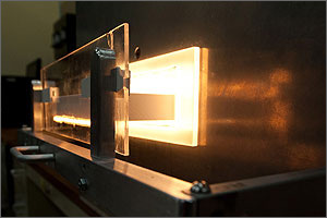
The cavity inside the Solar Optical Furnace glows white hot during a simulated firing of a solar cell.
Credit: Dennis Schroeder


Solar cells, the heart of the photovoltaic industry, must be tested for mechanical strength, oxidized, annealed, purified, diffused, etched, and layered.

Heat is an indispensable ingredient in each of those steps, and that's why large furnaces dot the assembly lines of all the solar cell manufacturers. The state of the art has been thermal or rapid-thermal-processing furnaces that use radiant or infrared heat to quickly boost the temperature of silicon wafers.

Now, there's something new.

A game-changing Optical Cavity Furnace developed by the U.S. Department of Energy's National Renewable Energy Laboratory uses optics to heat and purify solar cells at unmatched precision while sharply boosting the cells' efficiency.

The Optical Cavity Furnace (OCF) combines the assets that photonics can bring to the process with tightly controlled engineering to maximize efficiency while minimizing heating and cooling costs.

NREL's OCF encloses an array of lamps within a highly reflective chamber to achieve a level of temperature uniformity that is unprecedented. It virtually eliminates energy loss by lining the cavity walls with super-insulating and highly reflective ceramics, and by using a complex optimal geometric design. The cavity design uses about half the energy of a conventional thermal furnace because in the OCF the wafer itself absorbs what would otherwise be energy loss. Like a microwave oven, the OCF dissipates energy only on the target, not on the container.

Different configurations of the Optical Cavity Furnace use the benefits of optics to screen wafers that are mechanically strong to withstand handling and processing, remove impurities (called impurity gettering), form junctions, lower stress, improve electronic properties, and strengthen back-surface fields.

Making 1,200 Highly Efficient Solar Cells per Hour


NREL researchers continue to improve the furnace and expect it to be able soon to hike the efficiency by 4 percentage points, a large leap in an industry that measures its successes a half a percentage point at a time. "Our calculations show that some material that is at 16 percent efficiency now is capable of reaching 20 percent if we take advantage of these photonic effects," NREL Principal Engineer Bhushan Sopori said. "That's huge."

Meanwhile, NREL and its private-industry partner, AOS Inc., are building a manufacturing-size Optical Cavity Furnace capable of processing 1,200 wafers an hour.

At about a quarter to half the cost of a standard thermal furnace, the OCF is poised to boost the solar cell manufacturing industry in the United States by helping produce solar cells with higher quality and efficiency at a fraction of the cost.

The furnace's process times also are significantly shorter than conventional furnaces. The Optical Cavity Furnace takes only a few minutes to process a solar wafer.

NREL has cooperative research and development agreements with several of the world's largest solar-cell manufacturers, all intrigued by the OCF's potential to boost quality and lower costs.

R&D 100 Award Winner

NREL and AOS shared a 2011 R&D 100 Award for the furnace. The awards, from R&D Magazine, honor the most important technological breakthroughs of the year.

Billions of solar cells are manufactured each year. A conventional thermal furnace heats up a wafer by convection; a Rapid-Thermal-Processing furnace uses radiative heat to boost the temperature of a silicon wafer up to 1,000 degrees Celsius within several seconds.

In contrast to RTP furnaces, the Optical Cavity Furnace processing involves wafer heating at a relatively slower rate to take advantage of photonic effects. Slower heating has an added advantage of significantly lowering the power requirements and the energy loss, so it can boost efficiency while lowering costs.

"With all solar cells, optics has a big advantage because solar cells are designed to absorb light very efficiently," NREL Principal Engineer Bhushan Sopori said. "You can do a lot of things. You can heat it very fast and tailor its temperature profile so it's almost perfectly uniform."

In fact, the OCF is so uniform, with the help of the ceramic walls, that when the middle of the wafer reaches 1,000 degrees Celsius, every nook and cranny of it is between 999 and 1,001 degrees.

"The amazing thing about this is that we don't use any cooling, except some nitrogen to cool the ends of the 1-kilowatt and 2-kilowatt lamps," Sopori said. That, of course, dramatically lowers the energy requirements of the furnace.

The use of photons also allows junctions to be formed quicker and at lower temperatures.

As America strives to reach the goal of 80 percent clean energy by 2035, the White House and the U.S. Department of Energy are challenging the solar industry to reach the goal of $1 per watt for installed solar systems. To reach that goal, manufacturers need better, less expensive ways to make solar cells. At $250,000, the Optical Cavity Furnace can do more, do it quicker, and do it at a lower capital cost than conventional furnaces.

Twenty Years of Great Ideas

For more than two decades, Sopori had great ideas for making a better furnace.

He knew that incorporating optics could produce a furnace that could heat solar cells, purify them, ease their stress, form junctions and diffuse just the right amount of dopants to make them more efficient.

"It's always easy on paper," Sopori said recently, recalling the innovations that worked well on paper and in the lab, but not so well in the real world. "There are moments … you realize that no one has ever done something like this. Hopefully it will work, but there are always doubts."

Trouble was, he'd come up with some elegant theoretical solutions involving optics, but wasn't able to combine them with the optimal geometry and materials of a furnace. "We've had a whole bunch of patents (12) to do these things, but what we were missing was an energy-efficient furnace to make it possible," Sopori said.

And then, combining his expertise in optics with some ingenious engineering with ceramics, he had his ah-ha moment:

NREL's Optical Cavity Furnace uses visible and infrared light to uniformly heat crystalline silicon wafers, especially at the edges, which are prone to cooling or heat loss, at unprecedented precision. The rays heat the sample, but the wafer never physically contacts the lamps.

The Optical Cavity Furnace is versatile. Each step in the solar cell manufacturing process typically requires a different furnace configuration and temperature profile. However, with the OCF, a solar cell manufacturer simply tells a computer (using NREL proprietary software) what temperature profile is necessary for processing a solar cell.

So, the OCF can perform five different process steps without the retooling and reconfiguration required by the furnaces used today, all the while incrementally improving the sunlight-to-electricity conversion efficiency of each solar cell.


Source: National Renewable Energy Laboratory (NREL)

Solar Energy Shines brightly: Tapping that energy cost-effectively remains a challenge

MIT News
Oct 26, 2011

The sunlight that reaches Earth every day dwarfs all the planet’s other energy sources. This solar energy is clearly sufficient in scale to meet all of mankind’s energy needs — if it can be harnessed and stored in a cost-effective way.

Unfortunately, that’s where the technology lags: Except in certain specific cases, solar energy is still too expensive to compete. But that could change if new technologies can tip the balance of solar economics.

The potential is enormous, says MIT physics professor Washington Taylor, who co-teaches a course on the physics of energy. A total of 173,000 terawatts (trillions of watts) of solar energy strikes the Earth continuously. That’s more than 10,000 times the world’s total energy use. And that energy is completely renewable — at least, for the lifetime of the sun. “It’s finite, but we’re talking billions of years,” Taylor says.

Since solar energy is, at least in theory, sufficient to meet all of humanity’s energy needs, the question becomes: “How big is the engineering challenge to get all our energy from solar?” Taylor says.

Solar thermal systems covering 10 percent of the world’s deserts — about 1.5 percent of the planet’s total land area — could generate about 15 terawatts of energy, given a total efficiency of 2 percent. This amount is roughly equal to the projected growth in worldwide energy demand over the next half-century.

Such grand-scale installations have been seriously proposed. For example, there are suggestions for solar installations in the Sahara, connected to Europe via cables under the Mediterranean, that could meet all of that continent’s electricity needs.

Because solar installations of all types are modular, the experience gained from working with smaller arrays translates directly into what can be expected for much larger applications. “I’m a big fan of large-scale solar thermal,” says Robert Jaffe, the Otto (1939) and Jane Morningstar Professor of Physics. “It may be the only renewable technology that can be deployed at very large scale.”

And we do know how to harness solar energy, even at a colossal scale. “There’s no showstopper, it’s just a matter of price,” says Daniel Nocera, the Henry Dreyfus Professor of Energy at MIT.

Nocera foresees a time when every home could have its own self-contained system: For instance, photovoltaic panels on the roof could run an electrolyzer in the basement, producing hydrogen to feed a fuel cell that generates power. All the necessary ingredients already exist, he says: “I can go on Google right now, and I can put that system together.” Nocera’s own invention, a low-cost system for producing hydrogen from water, could help over the next few years to make such systems cost-competitive.
To read more click here...

Related Information:

Making sodium-ion batteries that are worth their salt

Engineerblogger
Oct 26, 2011

Argonne chemist Christopher Johnson holds a sodium-ion cathode.


Although lithium-ion technology dominates headlines in battery research and development, a new element is making its presence known as a potentially powerful alternative: sodium.

Sodium-ion technology possesses a number of benefits that lithium-based energy storage cannot capture, explained Argonne chemist Christopher Johnson, who is leading an effort to improve the performance of ambient-temperature sodium-based batteries.

Perhaps most importantly, sodium is far more naturally abundant than lithium, which makes sodium lower in cost and less susceptible to extreme price fluctuations as the battery market rapidly expands.

"Our research into sodium-ion technology came about because one of the things we wanted to do was to cover all of our bases in the battery world," Johnson said. "We knew going in that the energy density of sodium would be lower, but these other factors helped us decide that these systems could be worth pursuing."


Sodium ions are roughly three times as heavy as their lithium cousins, however, and their added heft makes it more difficult for them to shuttle back and forth between a battery's electrodes. As a result, scientists have to be more particular about choosing proper battery chemistries that work well with sodium on the atomic level.

While some previous experiments have investigated the potential of high-temperature sodium-sulfur batteries, Johnson explained that room-temperature sodium-ion batteries have only begun to be explored. "It's technologically more difficult and more expensive to go down the road of sodium-sulfur; we wanted to leverage the knowledge in lithium-ion batteries that we've collected over more than 15 years," he said.

Because of their reduced energy density, sodium-ion batteries will not work as effectively for the transportation industry, as it would take a far heavier battery to provide the same amount of energy to power a car. However, in areas like stationary energy storage, weight is less of an issue, and sodium-ion batteries could find a wide range of applications.

"The big concerns for stationary energy storage are cost, performance and safety, and sodium-ion batteries would theoretically perform well on all of those measures," Johnson explained.

All batteries are composed of three distinct materials—a cathode, an anode and an electrolyte. Just as in lithium-ion batteries, each of these materials has to be tailored to accommodate the specific chemical reactions that will make the battery perform at its highest capacity. "You have to pick the right materials for each component to get the entire system to work the way it's designed," Johnson said.

To that end, Johnson has partnered with a group led by Argonne nanoscientist Tijana Rajh to investigate how sodium ions are taken up by anodes made from titanium dioxide nanotubes. "The way that those nanotubes are made is very scalable—if you had large sheets of titanium metal, you can form the tubes in a large array," Johnson said. "That would then enable you to create a larger battery."

The next stage of the research, according to Johnson, would involve the exploration of aqueous, or water-based, sodium-ion batteries, which would have the advantage of being even safer and less expensive.

Source: Argonne National Laboratory

Restraint Improves Dielectric Performance, Lifespan

Engineerblogger
Oct 26, 2011


Xuanhe Zhao


Just as a corset improves the appearance of its wearer by keeping everything tightly together, rigidly constraining insulating materials in electrical components can increase their energy density and decrease their rates of failure.

Many electrical components, like wiring, are typically surrounded by a material that keeps the electricity from passing to its surroundings. These insulating materials are known as dielectrics, and can take many forms, with the most common being “soft” materials known as polymers. However, since these dielectrics are constantly being submitted to electrical voltage, they tend to break down.

Duke University engineers have demonstrated that rigidly constraining dielectric materials can greatly improve their performance and potentially lengthen their lifespans. This insight follows their discovery earlier this year of the exact mechanism that causes soft dielectric materials to break down in the presence of electricity.


“We found that increasing voltage can cause polymers to physically crease and even crater at the microscopic level, eventually causing them to break down,” said Xuanhe Zhao, assistant professor of mechanical engineering and materials science at Duke’s Pratt School of Engineering. “So we thought if we wrapped the polymer tightly, that would prevent this creasing from occurring. Experiments proved this hypothesis to be true.”

The results of the Duke study were published online in the journal Applied Physical Letters.

In their experiments, the Duke researchers constrained three different soft polymer dielectrics with epoxy. Epoxy is a type of polymer created by the reaction of a resin with a hardening agent. When mixed, a hard and inflexible coating is formed.

“The rigid epoxy acts as a mechanical constraint,” Zhao said. “Since it adheres tightly to the dielectric, it prevents the deformation that would normally occur. We found that this constraint can greatly enhance the ability of the component to carry greater voltage, increasing its energy density by more than ten times.”

Zhao said that scientists have been working for years to develop new dielectrics based on new types of soft materials or polymers to increase energy density and solve the problem of breakdown.

“We believe that there can be a drastically different approach to achieving these higher energy-dense soft dielectrics,” Zhao said. “Our experiments show that the energy density of these soft materials can be significantly enhanced by proper mechanical constraints of the dielectrics, and not necessarily a new type of dielectric material.”

The team is currently testing newer methods for achieving even tighter constraints to increase the energy density of polymer dielectrics.

Source: Duke Unviersity

German lessons don't sink in

The Engineer
Oct 26, 2011

Companies like BMW embody the strengths of the German philosophy of education of engineers and reap the benefits of investment in early-stage technologies

It sometimes seems that every editorial comment we write at The Engineer ends up with a call for more funding from government in something or other. A quick check back on my previous pieces show that it’s not quite every one — but very nearly.

I make no apologies for that. The shortsighted approach by government to investment in science and technology is one of the UK’s major failings, and has been for many years.

A piece by veteran journalist and author John Kampfner in today’s Guardian hit the nail on the head. Kampfner, the newspaper’s former German correspondent, is discussing the differing attitude to labour laws in Germany and the UK, but early in the article he hits the nail on the head concerning the view of the importance of technology and engineering, and on funding them, in the two countries.

German economic strength, he says, is based not based on ‘cyclical, unsustainable factors’ such as property booms. ‘Instead, the German — and broader north European — approach emphasises vocational training and apprenticeships, particularly in engineering, manufacturing and the sciences. It invests in research and development, and in strong education.’

It would be wrong to portray Germany as a paradaisical haven for engineers and engineering. Chat to a German technology journalist and you’ll hear as much concern about skills gaps, government indecision and inertia, and even about the waning status of engineers. But despite this, Germany just seems to get it right more often than the UK. From the success of the Fraunhofer Institutes — which we’re only just starting to emulate, over forty years after they were set up — to the ingrained importance of engineering careers, Germany consistently sets the pace in industrial innovation.
To read more click here...

Engineers bring new meaning to the force of light

Engineerblogger
Oct 26, 2011

Yale University engineers recently demonstrated that nanomechanical resonators can operate at much higher amplitudes than previously thought. The results represent an advance in optomechanics, in which the force of light is used to control mechanical devices, and could have implications for future communications and sensing technologies.


New research by engineers at the Yale School of Engineering & Applied Science demonstrates that nanomechanical resonators can operate at much higher amplitudes than previously thought. The results represent an advance in optomechanics, in which the force of light is used to control mechanical devices. The findings could have implications for future communications and sensing technologies.

“We can flip a tiny switch with light,” said Hong Tang, associate professor of electrical engineering at Yale and the principal investigator of a new paper appearing online Oct. 23 in the journal Nature Nanotechnology.

Amplitude refers to vibration range. Achieving high-amplitudes in traditional nanoscale mechanical systems has proven difficult because reducing a resonator’s dimensions generally limits how much the resonator can move. Tang’s team shows a way of overcoming the performance limitations of conventional systems.

The operating principle is similar to the laser cooling technique used in atomic physics. “One can control the motion of a mechanical structure, amplify or cool its vibrations, just by controlling the wavelength of laser light,” said Mahmood Bagheri, the postdoctoral associate in Tang’s lab who is the paper’s lead author.

Tang and his research team also demonstrate in the paper that a tiny silicon structure within an optomechanical system can effectively store information without the aid of steady power supply — thus serving as a mechanical memory device.

Among other benefits, optomechancial memory devices can withstand harsher environments than electronic or magnetic memory devices, without losing data. Future technologies containing similar high-amplitude optomechanical resonators might be less sensitive to environmental conditions, such as variations in temperature and radiation. At the same time, high-amplitude resonators might enable more accurate and robust measuring devices.

Source: Yale University

Tuesday 25 October 2011

Solar Ship: The aircraft transport without dependency

Engineerblogger
Oct 25, 2011


There has been resurgence of interest in airships for military and commercial such as the High Altitude Long Endurance-Demonstrator (HALE-D) by Lockheed Martin's and Hybrid Air Vehicles (HAV) heavy-lift variant of Northrop Grumman's Long-Endurance Multi-Intelligence Vehicle (LEMV). Similar to HAV's design, this concept from the Canadian based company Solar Ship is a hybrid airship which relies on aerodynamics to help provide lift, and like the HALE-D, it would have its top surface area covered in solar cells to provide energy and minimize its carbon footprint.

Although the Solar Ship aircraft would be filled with helium, under normal circumstances they would rely on the aerodynamic lift provided by their wing shape to provide more than half the lift required to get them off the ground. Additionally, the aircraft could also fly when filled with plain old air. Jay Godsall, Solar Ship's founder, told the Toronto Star that the aircraft will be able to go where there's no roads, no airstrips, and where planes and helicopters can't reach on a tank of fuel.

Solar Ship says the aircraft's electric motor can either be powered solely by the energy provided by the on board batteries, or by the photovoltaic cells covering the top surface of the wing.  This feature has already been achieved by a conventional airplane design in the form of Solar Impulse.

The company points out that such heavier-than-air airships provide numerous advantages over their lighter-than-air brethren. Firstly, no mooring infrastructure or ballast weight is required to keep the aircraft from floating away during loading or unloading, making them more practical for the remote locations in which they are designed to operate. Additionally, not relying on buoyancy for lift means the aircraft can be smaller than lighter-than-air aircraft carrying the same payload. They are also more structurally robust and more maneuverable and resistant to wind and weather conditions.

Eventually, three sizes of craft will be on offer - a small Caracal, a medium-sized Chui, and a whopping great big hauler Nanuq, which is designed to carry payloads of up to 30 tonnes (66,139 lb).

Solar Ship has already built and flown a 10 m (33 ft) prototype.  Further tests and demonstrations of the craft will be conducted in summer 2013, with a test of a smaller ship due in late 2012 in Africa. The videos provides a glimpse of the company's vision for the future in which it sees a wide range of uses for its heavier-than-air aircraft, from delivery of urgent medical supplies to remote communities and disaster relief, to environmental monitoring and military applications.