Construction management experts at the University of Calgary's Schulich School of Engineering have developed a system that employs remote sensing technology to improve safety on construction sites by using tracking tags to monitor movements in real-time. Knowing the precise location of people, equipment and building materials will reduce accidents and could also help prevent materials from being placed too close to edges where they could fall.
Civil engineering professor Farnaz Sadeghpour and graduate student Reza Maalek developed the new tool, which uses Ultra Wide-Band signals, a type of radio frequency technology.
"Most construction accidents happen because of workers clashing with equipment and people or objects falling off edges. Our system will address both," says Sadeghpour, assistant professor in the Department of Civil Engineering at the Schulich School of Engineering.
While the tool is still under development, researchers plan to enable the system to trigger an alarm when someone gets too close to a certain piece of equipment or when a worker or a piece of building material gets too close to an edge. The warning could come in the form of an alert on a mobile phone or an urgent announcement on a worksite.
In 2009, a three-year-old girl was killed when a sheet of corrugated steel fell from a Calgary office tower that was under construction. A tracking system would help ensure materials are properly secured and kept a safe distance away from open thresholds. Other advantages include inventory and theft control. Removing an item from a site without authorization, for example, would trigger an alarm.
Ultra Wide-Band technology is becoming less expensive all the time and it could one day be widely used by industry as a cost-effective way to track important and valuable items.
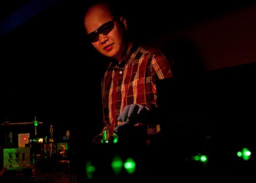
Strong attraction that arises between biological objects with random patches of electric charge on an otherwise neutral surface may partly explain pattern recognition in biology.
Theoretical physicist Ali Naji from the IPM in Tehran and the University of Cambridge, UK, and his colleagues have shown how small random patches of disordered, frozen electric charges can make a difference when they are scattered on surfaces that are overall neutral. These charges induce a twisting force that is strong enough to be felt as far as nanometers or even micrometers away. These results, about to be published in EPJ E¹, could help to understand phenomena that occurr on surfaces such as those of large biological molecules.
To measure the strength of the twist that acts on a randomly charged surface, the authors used a sphere which was mounted like a spinning top next to a randomly charged flat substrate. Because small amounts of positive and negative charges were spread in a disordered mosaic throughout both surfaces, they induced transient attractive or repulsive twisting forces. This was regardless of the surfaces’ overall electrical neutrality, thus making the sphere spin. Using statistical averaging methods, the authors studied the fluctuations of these forces.
The authors found that the twisting force, created by virtue of the disorder of surface charges, is expected to be much stronger and far-reaching than the remnant forces. The latter are always present, even in the absence of charge disorder, and are due to fluctuations at the atomic and molecular levels.
This could have implications for large randomly charged surfaces such as biological macromolecules, which may be exposed to strong electrostatic forces, inducing attraction and/or repulsion, even if they carry no overall net charge. For instance, this phenomenon could partly explain biological pattern recognition, such as lock and key phenomena. In that context, the twisting force could explain the attraction between biological macromolecules that lead to pre-alignment prior to their interaction.
Minute-scale interactions govern electronic behaviour of superconductors with potential applications for voltage measurement techniques.
Researchers studying a superconducting strip observed an intermittent motion of magnetic flux which carries vortices inside the regularly spaced weak conducting regions carved into the superconducting material. These vortices resulted in alternating static phases with zero voltage and dynamic phases, which are characterised by non-zero voltage peaks in the superconductor. This study, which is about to be published in EPJ B¹, was carried out by scientists from the Condensed Matter Theory Group of the University of Antwerp, Belgium, working in collaboration with Brazilian colleagues.
Superconductors, when subjected to sufficiently strong magnetic fields, feature vortices that carry quantized amounts of magnetic flux, although the natural tendency of superconductors is to expel such flux. The authors relied on the Ginzburg-Landau theory to study the dynamic of the nanometric- to millimetric-scale-width superconducting strip, which was subjected to a magnetic field applied at a right angle and a current applied alongside its length.
Typically, weakly acting superconducting regions are natural impediments for the passage of electrical current. However, the authors found that they also work as efficient pathways for vortices to enter and exit the superconducting strip. The increasing magnetic field also increases the density of mutually repelling vortices, which stimulates vortex motion across the strip in the presence of an external current. At the same time, the barrier for vortex entry and exit on the strip boundaries is also dependent on the magnetic field. This interplay of magnetic-field-dependent barriers and vortex-vortex interaction results in an on/off vortex motion in increasing magnetic fields.
Due to the simple geometry of the strip, these results can be confirmed experimentally in magnetoresistance measurements. These findings could be applicable in gate devices used to control various modes of on/off states in electrical systems which operate in specific windows of temperature, applied magnetic field, current and voltage.
Offshore options: there are four main types of wind turbine foundations — monopile, jacket, tripile and gravity base.
Solid foundations: onshore assembly could enable serial production of offshore wind turbines
When Germany announced that it was effectively turning its back on nuclear power by mothballing all of its reactors by 2022, there were more than a few surprised faces and some awkward questions.
How exactly did the country think it was going to meet its energy needs? Surely it would have to import considerable amounts from neighbouring France, thereby subscribing to nuclear by proxy.
The answer was perhaps even more surprising. On 1 January this year, the German parliament enshrined into law an act requiring that by 2020 35 per cent of all of its energy needs must be provided by renewable sources, followed by 50 per cent by 2030 and 80 per cent by 2050 — far more ambitious in scope and magnitude than the European Union’s target of 20 per cent by 2020.
Germany was already making good progress in the sector, particularly with offshore wind and geothermal energy. There are currently eight operational offshore wind farms, generating around 200MW. To meet the first set of 2020 targets, though, calls for upwards of 10GW.
Clearly there needs to be a complete step-change in production; a few parks going up here and there every decade or so simply won’t cut it.
Europe’s largest construction company, the Austro-German group Strabag, started dabbling in the offshore wind business around 10 years ago, focusing on its existing strengths of production, transport and installation. It also began experimenting with new designs for base foundations, believing that this was a key limiting factor the overall production chain in offshore wind.
Essentially there are around four main types of wind turbine foundations in use(image above).
When turbines took their first tentative steps from land into the shallow waters just off the coast, they generally employed monopile foundations — a simple design in which the wind tower is supported by a steel pipe, either directly or through a transition piece.
Depending on the subsurface conditions, the pile is typically driven into the seabed by either large impact or vibratory hammers, or the piles are grounded into the sockets drilled into rock. They are reasonably cost effective but not suited to water depths of more than 15m and they struggle to hold turbines greater than 2-3MW.
To handle some of the latest generation of 5-10MW wind turbines, moored in greater water depths many miles off the shore, requires a bit more support. Jacket foundations consist of a frame construction similar to an electricity pylon. It is technology essentially borrowed straight from the oil industry.To read more click here...
Utilizing this new method, Taylor was able to demonstrate a solar cell platform, a lithium battery, and a fuel cell membrane electrode assembly, all with good performance. Credit: Yale University
A key problem in materials science is balancing the trade-offs
between different material properties: improving one property can have a
negative impact on others. Synthetic composites are often used to
address this problem. Designed to offer more independently “tunable”
performance, these composites take advantage of multiple materials’
properties within a single system, and have various applications,
including photovoltaic, battery and fuel cell technology.
Single-walled carbon nanotubes (SWNTs) have unique and
extraordinary properties that make them popular as starting points for
synthetic composites, used in combination with polymers. Yet these
nanotubes present their own challenges. When combined with a polymer,
they often spread poorly, resulting in a composite with a meager
conductivity in comparison to a pure SWNT network. The current
techniques used to overcome this problem limit themselves to the use of
conductive polymers that often do not disperse SWNTs well, which
dramatically limits the design freedom and extended applications of
composite materials.
Professor André Taylor,
Director of the Transformative Materials & Devices group at Yale
SEAS, has developed a scalable tandem Mayer rod coating technique that
preserves the electrical properties of these nanotubes when fabricating
SWNT and polymer composites. This novel approach eliminates the need to
use functional polymers that are capable of properly spreading the SWNTs
and thus loosens the design limitations for developing advanced
multifunctional composites.
Instead of immediately spreading the nanotubes within the desired
polymer for the final composite, the SWNTs are first dispersed using a
polymeric derivative of cellulose, sodium carboxymethyl cellulose (CMC).
The resulting film, which is transparent and contains well-dispersed
SWNTs suspended throughout the CMC, is coated onto glass slides. It is
transparent, but due to the CMC, nonconductive.
Conductivity is restored in the next step of the group’s technique,
where the CMC is removed by treating the film with acid. Removing the
CMC lets the nanotubes collapse onto each other, creating a dense
network of connected nanotubes with high conductivity. With this highly
conductive network of SWNTs on which to base a composite system, a
functional polymer can be selected and filled into the network based on
the intended application. The resulting films offer exceptional
electrical performance from the nanotube network and can be customized
for additional desired properties based the polymer that’s selected for
use.
Xiaokai Li, the lead author of the paper, states, “As the
challenges of generating more complex SWNT-based film systems require
engineers to impart new and transformative functionalities to materials
without sacrificing the conductivity or ease of manufacturing, our
technique provides the versatility to control nanoscale features and
functionality on the macroscopic level.”
What is truly unique about this approach, says Taylor, is that the
group was able to demonstrate a solar cell platform, a lithium battery,
and a fuel cell membrane electrode assembly, all with good performance.
“Normally these systems are made from individual layers, but by
using this tandem Mayer rod coating approach, we have been able to
create films that are asymmetric: electrically conductive on one side
dominated by the SWNT network and functional polymer (for ion transport,
etc.) on the other,” says Taylor. “This opens up a new range of
possibilities for advanced functional composites.”
The group’s next step is to design and process carbon nanotube
composite films using the same method specifically for next generation
flexible heterojunction solar cells.
Funding from the Semiconductor Research Corporation and the National Science Foundation supported this work.
Vertical-cavity surface-emitting laser Colloidal
quantum dots — nanocrystals — can produce lasers of many colors. Cuong
Dang manipulates a green beam that pumps the nanocrystals with energy,
in this case producing red laser light. Credit: Mike Cohea/Brown University
Engineers at Brown University and QD Vision Inc. have created nanoscale single crystals that can produce the red, green, or blue laser light needed in digital displays. The size determines color, but all the pyramid-shaped quantum dots are made the same way of the same elements. In experiments, light amplification required much less power than previous attempts at the technology. The team’s prototypes are the first lasers of their kind.
Red, green, and blue lasers have become small and cheap enough to find their way into products ranging from BluRay DVD players to fancy pens, but each color is made with different semiconductor materials and by elaborate crystal growth processes. A new prototype technology demonstrates all three of those colors coming from one material. That could open the door to making products, such as high-performance digital displays, that employ a variety of laser colors all at once.
“Today in order to create a laser display with arbitrary colors, from white to shades of pink or teal, you’d need these three separate material systems to come together in the form of three distinct lasers that in no way shape or form would have anything in common,” said Arto Nurmikko, professor of engineering at Brown University and senior author of a paper describing the innovation in the journal Nature Nanotechnology. “Now enter a class of materials called semiconductor quantum dots.”
The materials in prototype lasers described in the paper are nanometer-sized semiconductor particles called colloidal quantum dots or nanocrystals with an inner core of cadmium and selenium alloy and a coating of zinc, cadmium, and sulfur alloy and a proprietary organic molecular glue. Chemists at QD Vision of Lexington, Mass., synthesize the nanocrystals using a wet chemistry process that allows them to precisely vary the nanocrystal size by varying the production time. Size is all that needs to change to produce different laser light colors: 4.2 nanometer cores produce red light, 3.2 nanometer ones emit green light and 2.5 nanometer ones shine blue. Different sizes would produce other colors along the spectrum.
The cladding and the nanocrystal structure are critical advances beyond previous attempts to make lasers with colloidal quantum dots, said lead author Cuong Dang, a senior research associate and nanophotonics laboratory manager in Nurmikko’s group at Brown. Because of their improved quantum mechanical and electrical performance, he said, the coated pyramids require 10 times less pulsed energy or 1,000 times less power to produce laser light than previous attempts at the technology.
Quantum nail polish
When chemists at QDVision brew a batch of colloidal quantum dots for Brown-designed specifications, Dang and Nurmikko get a vial of a viscous liquid that Nurmikko said somewhat resembles nail polish. To make a laser, Dang coats a square of glass — or a variety of other shapes — with the liquid. When the liquid evaporates, what’s left on the glass are several densely packed solid, highly ordered layers of the nanocrystals. By sandwiching that glass between two specially prepared mirrors, Dang creates one of the most challenging laser structures, called a vertical-cavity surface-emitting laser. The Brown-led team was the first to make a working VCSEL with colloidal quantum dots.
The nanocrystals’ outer coating alloy of zinc, cadmium, sulfur and that molecular glue is important because it reduces an excited electronic state requirement for lasing and protects the nanocrystals from a kind of crosstalk that makes it hard to produce laser light, Nurmikko said. Every batch of colloidal quantum dots has a few defective ones, but normally just a few are enough to interfere with light amplification.
Faced with a high excited electronic state requirement and destructive crosstalk in a densely packed layer, previous groups have needed to pump their dots with a lot of power to push them past a higher threshold for producing light amplification, a core element of any laser. Pumping them intensely, however, gives rise to another problem: an excess of excited electronic states called excitons. When there are too many of these excitons among the quantum dots, energy that could be producing light is instead more likely to be lost as heat, mostly through a phenomenon known as the Auger process.
The nanocrystals’ structure and outer cladding reduces destructive crosstalk and lowers the energy needed to get the quantum dots to shine. That reduces the energy required to pump the quantum dot laser and significantly reduces the likelihood of exceeding the level of excitons at which the Auger process drains energy away. In addition, a benefit of the new approach’s structure is that the dots can act more quickly, releasing light before Auger process can get started, even in the rare cases when it still does start.
“We have managed to show that it’s possible to create not only light, but laser light,” Nurmikko said. “In principle, we now have some benefits: using the same chemistry for all colors, producing lasers in a very inexpensive way, relatively speaking, and the ability to apply them to all kinds of surfaces regardless of shape. That makes possible all kinds of device configurations for the future.”
In addition to Nurmikko and Dang, another author at Brown is Joonhee Lee. QD Vision authors include Craig Breen, Jonathan Steckel, and Seth Coe-Sullivan, a company co-founder who studied engineering at Brown as an undergraduate.
The US. Department of Energy, the Air Force Office for Scientific Research, and the National Science Foundation supported the research. Dang is a Vietnam Education Foundation (VEF) Scholar.
University of Exeter researchers Dr Monica Craciun and Dr Saverio Russo.
The most transparent, lightweight and flexible material ever for conducting electricity has been invented by a team from the University of Exeter.
Called GraphExeter, the material could revolutionise the creation of wearable electronic devices, such as clothing containing computers, phones and MP3 players.
GraphExeter could also be used for the creation of ‘smart’ mirrors or windows, with computerised interactive features. Since this material is also transparent over a wide light spectrum, it could enhance by more than 30% the efficiency of solar panels.
Adapted from graphene, GraphExeter is much more flexible than indium tin oxide (ITO), the main conductive material currently used in electronics. ITO is becoming increasingly expensive and is a finite resource, expected to run out in 2017.
These research findings are published in Advanced Materials, a leading journal in materials science.
At just one-atom-thick, graphene is the thinnest substance capable of conducting electricity. It is very flexible and is one of the strongest known materials. The race has been on for scientists and engineers to adapt graphene for flexible electronics. This has been a challenge because of its sheet resistance, which limits its conductivity. Until now, no-one has been able to produce a viable alternative to ITO.
To create GraphExeter, the Exeter team sandwiched molecules of ferric chloride between two layers of graphene. Ferric chloride enhances the electrical conductivity of graphene, without affecting the material’s transparency.
The material was produced by a team from the University of Exeter’s Centre for Graphene Science. The research team is now developing a spray-on version of GraphExeter, which could be applied straight onto fabrics, mirrors and windows.
Lead researcher, University of Exeter engineer Dr Monica Craciun said: “GraphExeter could revolutionise the electronics industry. It outperforms any other carbon-based transparent conductor used in electronics and could be used for a range of applications, from solar panels to ‘smart’ teeshirts. We are very excited about the potential of this material and look forward to seeing where it can take the electronics industry in the future.”
The Centre for Graphene Science brings together the Universities of Exeter and Bath in internationally-leading research in graphene. The Centre is bridging the gap between the scientific development and industrial application of this revolutionary new technology.
This research was funded by the EPSRC and Royal Society.
Radio signals reach pilots on board an aircraft through the “radar dome“, the rounded nose of the aircraft. But if errors occur during the production of this “nose“, – tiny foreign particles, drops of water or air bubbles – this can impede radio traffic. In the future, a non-destructive testing system will identify just such imperfections during production. Researchers will be presenting the new testing system at the Control trade fair, May 8-11 in Stuttgart.
The planned arrival time, the request to land or the landing direction – this is the kind of information pilots discuss via radio with ground staff in the control tower. The nose of the aircraft, the „radar dome“, receives incoming radio signals and transmits radio signals sent by the pilot as well. It is made of a fiberglass composite. But if even tiniest imperfections arise during production – if, for instance, little foreign particles, drops of water or air bubbles become enclosed in the resin – over time they can cause fine cracks through which moisture can seep. This causes interference in radio traffic through the aircraft nose, introducing static into the signal.
As part of the Dotnac project, researchers at the Fraunhofer Institute for Physical Measurement Techniques IPM in Kaiserslautern are working with partners in industry and research to develop a new testing system: the system uses terahertz waves to completely scan the aircraft nose, which is several centimeters thick, and immediately identify any flaws. The frequency of terahertz waves falls between that of microwaves on the one hand and infrared light on the other. They are completely harmless to humans. The waves are generated in a rolling cabinet not unlike those found in many offices: it contains a microwave source and all electronics to control the system and to collect the data. A frequency mixer multiplies the frequency of the microwave radiation generated into the terahertz range. Researchers have connected the actual measurement module to this container by means of electrical wires. This module emits the terahertz waves toward the radar dome. The material reflects the radiation, and the detector integrated in this module analyzes the reflected terahertz radiation. If there are any air bubbles or little imperfections embedded in the material, they turn up in the reflected signal. The main challenge facing researchers was to find out which terahertz frequencies they would have to use to bombard the material to achieve the most effective results for the various imperfections. Higher frequencies create better resolution, while lower frequencies have less difficulty penetrating the material. The researchers select from a range of different frequencies depending on the errors the researchers are looking for in the case concerned. The scientists have already developed a prototype of the testing system. It will be presented at the Control trade fair, May 8-11, in Stuttgart. Around a year from now, the scanner will have advanced to the point that it will scan and analyze aircraft noses automatically. Thus far, simple scanners for level and rotations symmetrical objects are available.
Researchers have come up with another terahertz testing system as well, one that analyzes the thickness of layers – such as are found on aircraft and cars. “Our terahertz measuring system is one of the few robust enough for industrial use,“ according to Dr. Joachim Jonuscheit, deputy head of department at Fraunhofer IPM. Just like the system that checks aircraft noses, this one also consists of a rolling cabinet along with a transmitter and a receiver connected to the container by cables five meters long. This system works with very short terahertz pulses. Each pulse is partially reflected off of the interfaces of the layers: the surface of the first layer, the interface between layer one and two, and so on. The deeper the layer reflecting the pulses, the longer the pulses take to return to the detector. Using the time each pulse takes to make its way back to the detector, built-in software automatically calculates the thickness of the various layers.
The system‘s great advantage is its robustness. But how did researchers accomplish this? “First of all, we no longer shoot the laser that excites the system by open beam as typically used in terahertz systems; instead, we feed it through optical fibers. And secondly, we have fixed and arranged the optical elements to make them mechanically robust. We have also improved the manufacturing processes for the semiconductor components – the transmitters and detectors – to make the individual elements more resistant,“ Jonuscheit explains. At the Control trade fair, the researchers will demonstrate live measurements on multi-layered plastic films of varying thicknesses.
If errors creep in during the assembly of components, costly post-processing is often the consequence. Automatic testing is difficult, especially where individual products are concerned. Now there is a new testing system that is flexible and economical, even for smaller production runs. Researchers will be presenting the new technology at the Control trade fair, May 8-11 in Stuttgart.
Today‘s cars are increasingly custom-built. One customer might want electric windows, heated door mirrors and steering-wheel-mounted stereo controls, while another is satisfied with the minimum basic equipment. The situation with aircraft is no different: each airline is looking for different interior finishes – and lighting, ventilation, seating and monitors are different from one company to the next. Yet the customer‘s freedom is the manufacturer‘s challenge: because individual parts and mountings have to be installed in different locations along the fuselage, automated assembly is often not an economical alternative. For many assembly steps, manufacturers have to rely on manual labor instead. But if errors creep in – if, for instance, a bracket is mounted backwards or in the wrong place – correcting them can get expensive later on. The fuselage has to be reworked at great expense. Today, employees use design drawings to determine whether the individual parts have been attached properly, or else manufacturers use rigid and inflexible testing systems to check the part against comparison photos. This calls for an identical part for the template photo – and that can be difficult where one-off parts are concerned.
Now, researchers at the Fraunhofer Institute for Factory Operation and Automation IFF in Magdeburg have come up with a testing technology that is reliable and economic even for one-off production runs. “The automated visual testing system generates a digital template and uses it to compare with the assembled components. It reliably identifies any errors,“ points out Steffen Sauer, project manager for measuring and testing technology at IFF. First, an automated camera system takes hundreds of photos of individually assembled holders, load-bearing elements and parts on the inside of the fuselage shell. For every picture taken, the system determines the exact position of the camera relative to the fuselage shell. At the same time, the software generates the same shots again – but this time using a “virtual“ camera. So essentially it creates “photos“ using the data of the digital design model. The system compares the photos of real parts with the “virtual“ images. If the system detects any deviations – if, say, a bracket is backwards – it issues a warning. Parts that have not been installed properly are highlighted on the monitor screen. The interesting thing is these steps are completely automatic.
In addition to a two-dimensional check using the photos, the system can also check a completed aircraft fuselage in three dimension: as in the case of the photos, it uses design data to generate three-dimensional data that it then compares with measurements on the real assembly. Here, conventional 3D measurement methods are used to digitalize the components. “What‘s new about this system is that we convert specifications from the design models into images and 3D data that the system can then compare with the real images,“ explains Sauer.. The system also automatically draws up the testing plan: first, it identifies the best measuring position for every part to be tested. What is the best location from which to test the component in question? The system forwards the results to the robot, which in turn travels to the position identified, where it shoots the two or three-dimensional images. There is another advantage to this approach: this way, the system can react quickly and flexibly. The result is a continuous process, from design to the finished and assembled part.
The main challenge to researchers was to set up the virtual camera that uses design models to “photograph“ the as yet non-existent component. Another crunch point was to quickly and automatically locate the interesting areas from among the many millions of points in the three-dimensional images – to hunt down, in the mass of points, the tiny components such as brackets and holders, and to check to see whether they are properly fitted. The fields of application for this testing technology are diverse: the technology can be used wherever flexibility is required and individual parts frequently change. The only condition: design data must be available. Researchers will be presenting the new technology at the Control trade fair, May 8-11 in Stuttgart. The process will be ready to use by summer 2012.
Panasonic Corporation today announced it has developed an advanced radar technology for next-generation traffic safety systems that enables to detect humans and vehicles in a range of several tens of meters. This millimeter-wave radar technology allows for detecting objects outdoors in poor visibility conditions, such as night, rain and snow, as well as against the sunlight. When applied in traffic surveillance sensors located at intersections, this innovative technology will help increase automotive safety by detecting pedestrians and bicycles hidden in the driver's blind spots.
As accidents at intersections account for about a half of all traffic fatalities, preventive measures are required to avoid collisions there involving cars, pedestrians and cyclists. Panasonic's new radar technology enables traffic monitoring sensors at intersections to detect pedestrians and bicycles up to 40 meters ahead even at nighttime and under bad weather conditions that hinder the driver's visibility. By alerting the driver of the presence of pedestrians in the crosswalk or bicycles in blind spots, this technology helps to reduce the driver's burden and traffic accidents.
Panasonic's new automotive radar technology has overcome the difficulties with conventional millimeter-wave radar technologies; the advanced radar technology is capable of detecting humans and cars simultaneously in spite of the fact that human body reflects extremely weak radar signals compared with car body. This innovative radar technology has also achieved high detection performance with a range resolution of less than 50cm and an angular resolution of 5 degrees, which enables to detect pedestrians and vehicles. Furthermore, unlike optical and infrared cameras and laser sensors, whose detection performance can be significantly affected by visibility conditions, this new radar technology will not be subject to such conditions as nighttime, rain, snow or dense fog.
Panasonic has developed and incorporated the following new element technologies to realize the new millimeter-wave radar technology for automotive applications:
Coded pulse modulation technique that employs a newly designed
code sequence for pulse radar method to improve sensitivity
characteristics, thereby achieving extension of the detection
range and finding out small objects that have weak radar
reflection.
Adaptive antenna technique that combines radar beamforming
transmission and adaptive array antenna reception with signal
processing algorism for estimation of target direction, thereby
achieving high angle resolution even with a smaller antenna
compared with conventional one.
With regard to millimeter-wave radars, there presently exist radars for vehicle to measure distance to the vehicle in front. However, these radars cannot detect human body with high resolution due to very weak radar reflection of human body. In addition, an optical camera is commonly used as a traffic surveillance sensor. However, it cannot work well under certain conditions such as nighttime because it can provide almost the same information as the human eye can capture.
Panasonic has achieved the new radar technology as part of the "Research and Development Project for Expansion of Radio Spectrum Resources" supported by the Ministry of Internal Affairs and Communications of Japan. The company will demonstrate the technology at VTC (Vehicular Technology Conference) 2012-Spring (May 7 to 9 in Yokohama, Japan), using a test equipment with an experimental radio license.
On the new radar technology, Panasonic holds eighteen patents in Japan and six patents overseas including pending applications.
Cross-section of a new magnetoelectric composite sensor as scanned in an
electron microscope: piezoelectric material (bottom half) and
magnetostrictive material with integrated support layers (upper half). Photo: Christiane Zamponi
Up to now, the brain’s magnetic field is measurable only under technical laboratory conditions. This technique is therefore not feasible in terms of the broader medical use, although it would be significant for diagnosing numerous conditions such as epilepsy and dementia, or even for improving therapies such as deep brain stimulation for treating Parkinson’s disease. Three research teams at Kiel University (Germany) have now jointly developed a new type of magnetoelectric sensor, which is intended to allow the use of this important technology in the future. The scientific breakthrough: As opposed to conventional magnetoelectric measuring techniques, the new sensors operate at normal conditions. Neither cooling nor external magnetic bias fields are required. A new article in Nature Materials describes the design and properties of these so-called exchange biased magnetoelectric composite materials.
“Our composites with exchange biasing present an international milestone in the research of magnetoelectric materials”, says Professor Eckhard Quandt, senior author of the study and spokesperson of the Collaborative Research Centre 855 Magnetoelectric Composites – Future Biomagnetic Interfaces (CRC 855). “By eliminating the dependence on externally applied magnetic bias fields, we have removed a significant obstacle for the medical application of magnetoelectric sensors such as magnetocardiography and magnetoencephalography”. As the sensors do not affect one another due to their particular design, measuring arrays made up of hundreds of units are now conceivable. This would enable the production of flow maps of heart currents or brain waves.
The new composites consist of a complex sequence of around a hundred layers of material, each of which is only a few nanometres thick. The magnetoelectric sensors contain both magnetostrictive and piezoelectric layers which, on the one hand, deform due to a magnetic field to be measured and, as a result of this, at the same time produce electrical voltage which is used as the measuring signal. Enno Lage who has been working on the study since 2010 explains its background: “With the conventional magnetoelectric layer systems it is only possible to perform such highly sensitive measurements if the sensor is subjected to a bias magnetic field.
“What makes our composites so extraordinary are antiferromagnetic supporting layers made of manganese iridium, which act like magnetic fields inside the material", he adds. “This means that the bias field for the measurement is produced directly in the sensor and no longer needs to be provided externally.” A complete sensor is usually a few millimetres in size and contains a multi-layer of this new material, which is approximately a thousandth of a millimetre thick. The new composite materials have been produced in the recently established Kiel Nano Laboratory’s cleanroom. “These types of sensor systems can only be produced successfully in this particle-free environment", says Dr. Dirk Meyners, who is scientifically supervising Lage during the doctoral degree programme.
With this step in the development towards removing the dependence of magnetoelectric measurements on external magnetic bias fields, the working groups led by Lorenz Kienle, Reinhard Knöchel and Eckhard Quandt have achieved an important objective of the CRC 855, which has been supported by the German Research Foundation since January 2010. The CRC’s overall aim is to develop such new materials and to implement them into a fully functional, biomagnetic interface between men and the outside world. Quandt indicates future prospects: “Beyond the CRC’s opportunities, in the Cluster of Excellence Materials for Life, which is currently being reviewed, we could promote a range of further applications on the basis of these composites, for example, as sensors for non-invasive brain stimulation.”
Lage, E., Kirchhof, C., Hrkac, V., Kienle, L., Jahns, R., Knöchel, R., Quandt, E. and Meyners, D.: Exchange biasing of magnetoelectric composites, Nature Materials, doi:10.1038/nmat3306
In 2011, Amendment II partnered with the University of Utah's Nano Institute in order to develop the implementation of carbon nanotubes (CNT's) into body armor applications. The result was RynoHide, an unprecedented lightweight and flexible ballistic compound.
Nanotechnology begins at the molecular level. A single carbon nanotube is 1:100,000 the thickness of a sheet of newspaper and five times stronger than steel. RynoHide harnesses the power of carbon nanotechnology in conjunction with traditional soft body armor components.
RynoHide makes flexible armor stronger.
Traditional armor is designed to stop projectiles moving thousands of feet per second from penetration and back-face deformation. Back-face deformation is the bulge that occurs in the back of the armor from a projectile hitting the front without passing completely though. Traditional armor is designed to minimize these threats by using 20 to 30 layers of a high tensile strength synthetic aramid, such as Kevlar.
The acceptable back-face deformation limit for body armor, as set by the National Institute of Justice, is 44mm, or nearly two inches. RynoHide helps body armor achieve a back-face deformation level in the low 30's, without increasing the weight of the armor.
Less back-face deformation means less hurt on the body.
"That's a huge advantage for the user of the armor if they get hit," says R.G. Craig, President of Amendment II. "It could be the difference between a stay in the hospital or simply going home at the end of the day to your family." Such protection is achieved without compromise in comfort and convenience.
Amendment II is the exclusive developer of CNT enchanted protective body armor. This innovative approach to ballistic resistant compound production is accomplished through an intricate and highly technical manufacturing process. CNT's are applied to RynoHide elements at the thread level. Nanotechnology has been used in other industries such as computer research, and telecommunications, but nothing like this has ever taken place in the protective armor field.
RynoHide has already been used successfully as a compound of lightweight armor systems, military and law enforcement uniforms, vehicle armor, and in structural applications. The potential usage that RynoHide has to offer in many more applications is extensive.
Smart energy: Entrepreneur Bill Gross amid the solar-thermal concentrators of eSolar’s Sierra SunTower in 2009.
Credit: Andres Castañeda
Two talks at the TED conference this year formed, back to back, a sort of debate about the future of our planet. First, Paul Gilding gave a talk entitled "The Earth Is Full," about how we are using up all Earth's resources, with possibly devastating consequences. Next, X Prize creator Peter Diamandis gave a presentation entitled "Abundance," about how we will invent innovative ways to solve the challenges that loom before us.
I believe that we will need great ingenuity to enable our planet to provide successfully for more than seven billion human beings, let alone the nine billion that will probably inhabit it by 2050, and I believe that information technology will make this ingenuity possible. Because of fluid marketplaces and an ever more globalized economy, nearly every important resource is becoming scarcer and more costly. Evidence of this is seen in the price not only of oil but also of aluminum, concrete, wood, water, rare-earth elements, and even common elements like copper. Everything is getting more expensive because billions of people are trying creatively to repackage and consume these materials. But there is one resource whose price has consistently has gone down: computation.
The power, cost, and energy use involved in one unit of computation is declining at a more consistent, dependable rate than we have seen with any other commodity in human history. That declining cost curve must be tapped to lower energy prices—and I believe it will be. This will happen as people ask: To achieve my purpose (in designing whatever device or system), can I use more "atoms" or more "bits" (computation power)? The choice will have to be bits, because atoms are going up in price while bits are going down.
Here are a few examples. When designing a car, one can put a bit more effort into stronger, lighter-weight materials, which will increase energy efficiency but possibly drive up cost; or one can put a lot more effort into using computational power to run simulations that optimize the use of materials. Today, computational fluid dynamics allow a designer to accurately design a new shape of car, put it in a computer wind tunnel instead of a physical one, and test 1,000,000 body designs to improve fuel mileage by significant amounts. This was never before possible for those constructing vehicles.
In solar energy, large fields of mirrors or photovoltaic panels can be optimized to be lighter, more reliable, and more power-efficient by putting a $2 microprocessor in every panel. An onboard computer that lets each panel track the sun independently replaces previous systems that used more steel, bigger gears, and bigger gearboxes—basically, more materials. As little as 10 years ago, the computing power and sensors needed to build a closed-loop, sun-tracking solar panel might have cost $2,000, or more than the panel itself, and thus the system would not have been cost effective. But with computing costs coming down by a factor of 1,000 every 15 years, all kinds of new opportunities arise to improve system design.
At eSolar, one of our companies, we designed and built a utility-scale solar-thermal power plant with a huge amount of computation embedded into the field of mirrors. We reduced the size of the components, cut the installation expense, and drove the cost of the system down to nearly half what had been achieved before. This experience proved to me the feasibility of replacing atoms with bits.
The price reduction curve for computing is not over—it's continuing, and each year will open up further avenues for ingenuity. That is important because our current energy resources are not at all easy to compete with. Fuels that we dig out of the ground and burn are extremely cheap. They are, in effect, the concentrated storage of millions of years of sunlight falling on Earth. Ironically, the biggest component of energy costs is the expense of moving the fuel to consumers from where it's obtained—and transportation costs are mostly fuel, too. So we are in a kind of vicious cycle. The way to break free of fossil fuels is to introduce something new to our energy equation that isn't fuel.
I believe ingenuity in the form of information technology is the only variable that offers sufficient leverage. We need to replace a cheap, unsustainable form of energy with sustainable forms of energy that are equally cheap. The only way to compete with cheap fuels is to be more clever with computation; that is, to use as little of anything else as possible.
For years, aerospace engineers have been inspired by the natural
world, and many have built and flown biologically inspired vehicles.
Engineers at Lockheed Martin Advanced Technology Laboratories
(ATL), Cherry Hill, N.J., are designing, flying, and 3D printing
Samarai, a family of unmanned aerial vehicles (UAVs) that mimic the
shape of winged maple seeds—samaras—that float to the ground each
spring. The vehicles are structurally simple, and inherently stable in
flight.
Shahrukh Tarapore,
senior research scientist at Lockheed Martin Advanced Technology
Laboratories, examines the 3D-printed Samarai as he pulls it from the
Stratasys Dimension 3D printer. Image: Lockheed Martin Advanced
Technology Laboratories
Since 2009, Lockheed Martin ATL engineers have been producing and
flying Samarai using traditional materials and manual manufacturing.
However, the team is now investigating 3D printing to produce the
vehicles.
The research project has two goals. The team will explore whether or
not 3D printing can drastically reduce the time and costs required to
design and manufacture the small UAV. Also, the team plans to develop a
tool that takes specific mission objectives—such as flight duration—as
input and automatically produce a customized vehicle design that meets
these objectives. This research could go far beyond the Samarai
platform, as the technology could be extended to support other complex
systems.
3D printing also helps gain insight into how the Samarai wing design
affects flight characteristics. Single wing, or monowing, flight is not
well understood, and the rapid manufacturing of different designs
through 3D printing, combined with testing the different variants and
measuring resulting performance, enables rapid exploration of the flight
design space. To read more click here...
New Life for 3D Printing
The additive manufacturing industry is populated by a broad family of
technologies and some high-end systems can achieve impressive results
with metals and polymers. Developments in ceramics may soon make a big
impact. The low end of the market has recently been shaken up by the
entry of some very low-cost systems that are causing a lot of excitement
in the hobbyist market.
The first 3D-printed full jaw replacement was made in laser-sintered titanium by the Belgian
company LayerWise. Image: LayerWise
Metal parts made by laser sintering of powders top the list in
performance. A wide range of stainless and tool steels, titanium and
nickel alloys, and cobalt-chrome, as well as copper, aluminum, and
precious metals can all be formed in machines built by companies such as
EOS (Munich), Concept Laser (Lichtenfels, Germany), Renishaw Inc. (Wotton-under-Edge, U.K.), and Phenix Systems
(Riom, France). Metal parts are fully dense, with a uniform
microstructure due to the localized melting of a static powder bed.
Titanium parts meet American Society for Testing and Materials (ASTM) standards for wrought titanium and exceed the strength and toughness of cast materials.
Laser cladding systems, such as those built by Optomec (Albuquerque, N.M.) and POM Group Inc.
(Auburn Hills, Mich.), operate by jetting metal powders through a
nozzle directed at a focused laser spot. These systems are able to build
up parts from different metals in different locations, and are also
able to effect repairs on damaged parts.
Medical implants are a very lively market for additive manufacturing
metal parts. Recently, a complete lower jaw was fabricated in titanium
by the Belgian company LayerWise on an EOS machine, and
subsequently coated with a bioceramic by plasma spraying. Smaller
custom-fit cranial implants, as well as dental implants and copings, are
becoming more and more common.
More than 30 different systems make plastic parts of some type.
Unlike laser-sintered metals, polymeric parts generally don't meet the
same standards as conventionally processed materials. This shortcoming
has relegated most processes to design prototyping and display models.
The additive manufacturing industry was founded in the mid-1980s by 3D Systems,
Rock Hill, S.C., with a technology called stereolithography, which is
still one of the most widely used and profitable methods. It is
moderately fast, accurate, and very reliable. It is also laser-based,
but rather than directing the laser onto a bed of powder, the laser is
focused on the surface of a bath of photopolymer that is selectively
cured in layers. The resulting parts—mostly epoxies and acrylics—are
transparent and relatively tough. Stereolithography parts are useful for
displaying the internal components of assemblies. To read more click here...
Industrial robots could be used for more precise machine milling for things such as aerospace components, after recent trials of new technology.
One of the key goals of the near-complete European COMET project is to develop robots that can compete against five-axis machine tools.
‘Up to now the problem with robots has been that they’re not quite accurate enough; they’re somewhere in the 2–5mm range,’ said Roland Krain of project partner TEKS. ‘If you calibrate it you can probably get down to a millimetre but it’s still not quite good enough for machining.’
The major current obstacles for fully automated machining are play, mechanical flexibility, thermal effects and particularly backlash.
‘A lot of companies have got robots that handle parts that need to be milled, but if they want to do milling they have to spend between £90,000 and £150,000 on a five-axis machine tool,’ Krain said. ‘If we can add a high-quality spindle into the mix, the robot is already there and so suddenly you’ve got a milling solution for a fraction of the cost — if we can get the accuracy of course.
The cornerstone of this accuracy will be adaptive tracking, which is being developed in collaboration with COMET partner Nikon Metrology of Tamworth. It has devised a stepwise solution for increasing accuracy.
The first offline solution involves measuring the robot in more than 300 poses to determine where it deviates from where it should have been. That information is then fed back into the CAM software. When running, the software then compensates for backlash by driving the robot to what it thinks is the ‘wrong position’.
This can be complemented by an online, real-time system comprising three linear built-in charge coupled device (CCD) cameras with cylindrical lenses that measure the location of infrared LEDs mounted on the robot head. Essentially, it measures where the robot is, then checks where it should be and sends a compensation down to the robot controller in milliseconds.
Preliminary tests of these systems were performed last week in the UK demonstrating sub-1mm accuracy. The final phase of testing will be delivering case studies later this year such as machining the final leading edge of an aircraft wing and deburring parts on the turbine disk.
Meanwhile, TEKS is now exploring applications of COMET technology outside of industrial machining. One comes from the civil engineering sector for surveying quarries and mines using long-range laser scanning.
The new technology has proved difficult in that large amounts of rather unmanageable date are produced, which is difficult to visualise with existing computer hardware and software.
Using COMET technology, TEKS bypassed the computer to machine lightweight models of sites in polystyrene.
The main partners of the COMET project are BTU, Delcam, Nikon Metrology, Fraunhofer IPA, TEKS, SIR and AMRC Manufacturing.
Find out about the progress of the COMET project, which aims to overcome the challenges facing European manufacturing industries by developing innovative robot machining systems that are flexible, reliable and predictable with an average of 30% cost efficiency savings in comparison to machine tools.
Through a process involving thin layers of material deposited on a
surface and then selectively etched away, the MIT team produced a
surface covered with tiny cones, each five times taller than their
width. This pattern prevents reflections, while at the same time
repelling water from the surface.
Image: Hyungryul Choi and Kyoo-Chul Park
One of the most instantly recognizable features of glass is the way it reflects light. But a new way of creating surface textures on glass, developed by researchers at MIT, virtually eliminates reflections, producing glass that is almost unrecognizable because of its absence of glare — and whose surface causes water droplets to bounce right off, like tiny rubber balls.
The new “multifunctional” glass, based on surface nanotextures that produce an array of conical features, is self-cleaning and resists fogging and glare, the researchers say. Ultimately, they hope it can be made using an inexpensive manufacturing process that could be applied to optical devices, the screens of smartphones and televisions, solar panels, car windshields and even windows in buildings.
The technology is described in a paper published in the journal ACS Nano, co-authored by mechanical engineering graduate students Kyoo-Chul Park and Hyungryul Choi, former postdoc Chih-Hao Chang SM ’04, PhD ’08 (now at North Carolina State University), chemical engineering professor Robert Cohen, and mechanical engineering professors Gareth McKinley and George Barbastathis.
Photovoltaic panels, Park explains, can lose as much as 40 percent of their efficiency within six months as dust and dirt accumulate on their surfaces. But a solar panel protected by the new self-cleaning glass, he says, would have much less of a problem. In addition, the panel would be more efficient because more light would be transmitted through its surface, instead of being reflected away — especially when the sun’s rays are inclined at a sharp angle to the panel. At such times, such as early mornings and late afternoons, conventional glass might reflect away more than 50 percent of the light, whereas an anti-reflection surface would reduce the reflection to a negligible level.
While some earlier work has treated solar panels with hydrophobic coatings, the new multifunctional surfaces created by the MIT team are even more effective at repelling water, keeping the panels clean longer, the researchers say. In addition, existing hydrophobic coatings do not prevent reflective losses, giving the new system yet another advantage.
Other applications could include optical devices such as microscopes and cameras to be used in humid environments, where both the antireflective and anti-fogging capabilities could be useful. In touch-screen devices, the glass would not only eliminate reflections, but would also resist contamination by sweat.
Ultimately, if the cost of such glass can be lowered sufficiently, even car windows could benefit, Choi says, cleaning themselves of dirt and grit on the exterior surface of the windows, eliminating glare and reflections that can impair visibility, and preventing fogging on the interior surface.
The surface pattern — consisting of an array of nanoscale cones that are five times as tall as their base width of 200 nanometers — is based on a new fabrication approach the MIT team developed using coating and etching techniques adapted from the semiconductor industry. Fabrication begins by coating a glass surface with several thin layers, including a photoresist layer, which is then illuminated with a grid pattern and etched away; successive etchings produce the conical shapes. The team has already applied for a patent on the process.
Since it is the shape of the nanotextured surface — rather than any particular method of achieving that shape — that provides the unique characteristics, Park and Choi say that in the future glass or transparent polymer films might be manufactured with such surface features simply by passing them through a pair of textured rollers while still partially molten; such a process would add minimally to the cost of manufacture.
The researchers say they drew their inspiration from nature, where textured surfaces ranging from lotus leaves to desert-beetle carapaces and moth eyes have developed in ways that often fulfill multiple purposes at once. Although the arrays of pointed nanocones on the surface appear fragile when viewed microscopically, the researchers say their calculations show they should be resistant to a wide range of forces, ranging from impact by raindrops in a strong downpour or wind-driven pollen and grit to direct poking with a finger. Further testing will be needed to demonstrate how well the nanotextured surfaces hold up over time in practical applications.
Andrew Parker, a senior visiting research fellow at Oxford University’s Green Templeton College in the U.K. who was not involved in this work, says, “Multifunctional surfaces in animals and plants are common. For the first time, as far as I am aware, this paper learns a lesson in manufacturing efficiency from nature by making an optimized antireflective and anti-fogging device. … This is the way that nature works, and may well be the future of a greener engineering where two structures, and two manufacturing processes, are replaced by one.”
The research was funded by the Army Research Office through MIT’s Institute for Soldier Nanotechnology; the Air Force Office of Scientific Research; Singapore’s National Research Foundation through the Singapore-MIT Alliance for Research and Technology (SMART) Centre, and the Xerox Foundation. Park and Choi are recipients of fellowships from Samsung and the Kwanjeong Educational Foundation/STX Scholarship Foundation, respectively.
Defect as a
recipe for success: The images of the high-resolution transmission
electron microscope show the arrangement of the individual atoms in a
copper particle. The arrows indicate stacking faults and twin
boundaries. In the detailed image, the stacking fault can be recognized
by the fact that the atoms (white dots) deviate from the blue line from a
certain position. How strongly is indicated by the red arrow on the
yellow line in the lower part of the image. The defects in the crystal
structure are also noticeable on the surface of the particles and
increase the activity of the catalyst.
There is now one less mystery in chemical production plants. For many decades industry has been producing methanol on a large scale from a mixture of carbon dioxide and carbon monoxide, as well as hydrogen. An international team, including chemists from the Fritz Haber Institute of the Max Planck Society in Berlin, has now clarified why the catalyst used in this process - copper and zinc oxide particles and a small portion of aluminium oxide - works so well. They also discovered why this reaction accelerator has to be produced in the tried and tested way. The researchers established that defects in an as yet unknown combination with mixing of copper and zinc oxide at the catalyst’s surface are the reason why the catalysts are so active. These findings could make a contribution to further improving the catalyst, and also help researchers develop catalysts that convert pure carbon dioxide efficiently. These could be used to recycle the greenhouse gas that is produced when fossil fuels burn.
Recycling could provide an elegant way of, for example, solving the problem of the carbon dioxide emission from coal-fired power stations. It is not only the fact that the gas would then no longer heat up the climate; methanol could be used to replace at least part of fossil raw materials, but above all could be used to store regenerative energy. “A changeover to green energies is not possible without energy storage systems,” says Robert Schlögl, Director at the Fritz Haber Institute of the Max Planck Society. This is because the electricity generated by wind turbines and solar installations varies strongly and does not follow demand. The findings of the chemists at the Fritz Haber Institute and their team of researchers could contribute to the development of catalysts that efficiently convert carbon dioxide produced in the combustion of coal, gas or oil with hydrogen into methanol or other chemical energy storage systems.
The Berlin-based Max Planck researchers were joined by scientists from the Helmholtz Zentrum Berlin für Materialien und Energie (HZB), the SLAC National Accelerator Laboratory in Menlo Park, California, Stanford University and Südchemie AG in carrying out the work. The researchers studied the catalyst which industry is already using to produce 50 million tonnes of methanol annually. However, industry uses a mixture of carbon dioxide and carbon monoxide for the process, which is produced especially for this purpose from natural gas or coal. “Only when we understand why this catalyst works so well and why it must be produced in the tried and tested way will we be able to optimise it and further develop it for the conversion of pure carbon dioxide,” says Malte Behrens, who played a crucial role in clarifying the catalyst’s mystery.
Where do the molecules team up?
The industrial catalyst is composed of innumerable nanoparticles, some made of copper, some of zinc oxide and a small proportion of aluminium oxide; together they form a type of nanosponge. Malte Behrens and his colleagues have now identified the sites in the aggregate where carbon dioxide and carbon monoxide molecules combine with their hydrogen partners via various intermediate steps. Using images from a high-resolution transmission electron microscope (HRTEM) and neutron diffraction, which provides information on the crystal structure, the scientists discovered defects in the arrangement of the copper atoms in the nanoparticles. They subsequently employed quantum chemical computations to prove that some of the intermediate products preferred to adsorb at these defects. This means: The defects increase the catalyst’s activity, as its exact task is to promote the formation of these intermediate products.
In addition, the scientists discovered why the zinc oxide plays an important role in the mixture. They investigated the nanosponge with the synchrotron radiation from the Bessy II electron storage ring at the Helmholtz-Zentrum Berlin für Materialien und Energie using equipment which the Max Planck researchers had developed especially for the investigation of catalysts. They used the X-ray portion of this extremely intense radiation to follow what was happening chemically on the surface of the reaction accelerator when it came into contact with the reaction partners. In these analyses, and also on HRTEM images, they ascertained that zinc oxide also creeps over parts of the copper particles, and that some atoms in the copper surface are even replaced by zinc. This also makes the catalyst very active: calculations showed that some intermediate products of the reaction - in this case those containing oxygen - are more likely to bond to the zinc than to the copper.
It had long been assumed that the copper was the only catalytically active component. The catalysis research therefore concentrated on increasing its surface, as more molecules find room for the chemical transformation on the larger surface. For a long time, chemists assumed that the zinc oxide’s only role was as a spacer; it was to prevent the copper particles fusing with each other in the heat of the reaction. The zinc oxide particles also fulfil this role, but it has been known for some years that zinc oxide also exerts another influence. This is because, although similar sponge-like structures from copper and metals other than zinc also have a large surface, they come nowhere near to achieving the activity of the copper-zinc-aluminium system. “Different effects of the zinc oxide were discussed,” says Malte Behrens. “Our investigations are now helping to finally explain its role.”
Search for catalysts no longer trial and error
Since the scientists now know which structural details characterise the tried and tested catalyst for methanol synthesis, they now understand why it is so difficult to prepare the reaction accelerator. The catalyst is produced from solutions of copper and zinc salts in several steps. Chemists first produce a precursor of the catalyst by precipitating both metals as carbonates. “The pH value and the temperature at which the precursor is produced decide on the activity of the catalyst,” says Malte Behrens. “The catalyst has a chemical memory.” Now the chemist can also explain what the catalyst remembers: Only in the tried and tested process does the copper crystallise with small defects, and the zinc creep over and into the copper.
These results are not only relevant because they can assist in improving the methanol synthesis and trim it for the recycling of emissions. “Our work also shows that we will only really understand catalysts when we look at them in all their complexity,” says Robert Schlögl. Researchers have often studied the catalytic process of methanol synthesis, but always on idealised model systems. These are easier to investigate and to describe theoretically. However, it is precisely the decisive details, such as defects, that do not exist in them. Moreover, the findings represent a paradigm change in catalysis research. “Until now, new catalysts have usually been found using the trial and error method,” says Robert Schlögl. “Our work shows that we can understand catalysts and their manufacture in detail. This allows us to develop catalysts in the future in a rational way, namely on the drawing board, as well.”
Two lamps are brighter than one. This simple truism does not necessarily apply to lasers, as a team of scientists, led by the Vienna University of Technology found out. When one laser is shining and next to it another laser is turned on gradually, complex interactions between the two lasers can lead to a total shutdown and no light is emitted anymore. For technologies connecting the fields of electronics and photonics, this result may be very important. The new findings have now been published in the journal “Physical Review Letters”.
When switching on means switching off
“Imagine two light bulbs right next to each other, one of which is switched on. As you gradually turn on the second bulb by adjusting a dimmer switch, you expect the room to get brighter”, says Matthias Liertzer. He studied the behavior of coupled micro-lasers using computer simulations, together with Professor Stefan Rotter at the Institute for Theoretical Physics (TU Vienna). They were assisted by scientists from Princeton University, Yale University and the ETH Zurich.
To make a laser shine, it has to be “pumped” – it has to be supplied with energy, using light or electric current. If only one of two micro-lasers is pumped, only the pumped laser emits light. Surprisingly, pumping the second laser too does not necessarily increase the brightness of the coupled system. Supplying more energy can even reduce the brightness, until both lasers become dark. “When we saw that the two lasers can switch each other off completely, due to the coupling between them, we knew: either we made a mistake or this is a spectacular result”, says Stefan Rotter. In the meantime, the effect was confirmed in independent calculations by the co-authors from Yale.
Connecting Physics, Math and Electrical Engineering
Light consists of waves, and it is well known that waves can interfere and cancel each other out. The interplay between the two lasers, however, is more complicated than that: “This effect is not just about wave interference. It is a combination of interference and light amplification, which can lead to seemingly paradoxical effects”, says Matthias Liertzer. New methods, some of which were developed by mathematicians at TU Vienna, were necessary to solve the complicated equations which describe this problem. “The phenomenon is based on what mathematicians call exceptional points”, says Stefan Rotter. Exceptional points are special intersections of surfaces in complex spaces. “The appearance of such exceptional points in our laser equations can lead to a laser blackout. In this way we could connect a rather abstract mathematical structure to a measurable phenomenon”, says Rotter.
Light and Microelectronics
Electrical engineers at the Vienna University of Technology are now working on experiments with micro lasers, in which the theoretical predictions should be verified. Laser effects like this one are especially interesting, as they show new ways to connect microelectronics and laser technology. In today’s computers, information is transmitted by electric signals. Adding laser light could open up exciting new possibilities.
Cotton fabric after a vertical flame test, where a flame touches the fabric for 12 seconds. Credit: Texas A&M
A thin polymer coating developed by materials engineers at Texas A&M University could keep cotton clothing and polyurethane-foam-based furniture from going up in flames.
And the coating is environmentally friendly, too.
Dr. Jaime Grunlan, an associate professor in the Department of Mechanical Engineering, works with polymer nanocomposites that have properties similar to those of metals and ceramics — conducting electricity, for instance — while maintaining properties of polymers, such as low density.
In 2010, Grunlan’s development of a flame-resistant polymer coating got him some attention, as he fielded calls from the United States military, the cotton industry, mattress manufacturers and the Federal Aviation Administration, and from companies around the world.
New advancements in the area, however, should garner even more attention.
“We can now make cotton fabric that doesn’t burn at all,” Grunlan says.
Grunlan's technology — which has been reported in Science News, Chemical and Engineering News, Nature and Advanced Materials — involves covering every microscopic fiber in a fabric with a thin composite coating of two polymers that exhibit an intumescent effect, producing a protective carbon foam coating when exposed to high temperatures.
The thin films are about one-tenth of a micron thick, or about one-thousandth the thickness of a human hair, and are created with the layer-by-layer assembly technique in which the coating is deposited onto the surface of the fiber being coated. This layer-by-layer process allows Grunlan to control the thickness of the coating down to the nanometer level.
Grunlan says the technology will be suitable for clothing, including children's clothing; lab coats; and medical clothing for both doctors and patients. It can even be used in military camps, where a fire in a single tent can wipe out an entire camp.
But the technology's applications go far beyond just clothing and fabric. The coating could be used in foams, such as those found in sofas, mattresses, theatre and auditorium seats, airplane seat cushions, and building insulation.
Foam cut through the middle after being exposed to fire from a butane torch. Credit: Texas A&M
On polyurethane foam, a coating of chitosan (a natural material extracted from shrimp and lobster shells) and clay is deposited to eliminate melt dripping during burning. The nanocomposite mixture coats the interior walls of foam. The result is that when burned, the treated foam keeps its shape instead of puddling at high temperatures like untreated polyurethane foam does. This quality eliminates the “melt-dripping” effect that further spreads fires.
"It's like we're building a nano-brick wall within each cell of the foam," Grunlan says.
That brick wall keeps the foam from being destroyed. And the coating is so thin that it adds only 4 to 5 weight-percent to the foam and does not negatively alter its color, texture or flexibility.
"A lot of anti-flammables degrade fabric and foam properties," Grunlan says.
But with Grunlan's technique, each thread can be individually coated, in the case of cotton fabric. In fact, his coating could potentially strengthen fabric. The researchers are also looking at ways to make the coating softer and more durable to washing.
Current flame-retardant materials rely on brominated compounds, many of which have been banned due to concerns over their potential toxicity. The Texas A&M researchers were searching for an alternative to these toxic chemicals, and had previously been using a commonly known clay and a commercial synthetic polymer to make their coatings. But in order to make the coatings more sustainable, Grunlan switched to chitosan.
“Based on initial results,” he says, “I really think this is going to become a widely adopted, environmentally benign alternative to current flame retardant treatments.
"Anywhere you want to make fabric or foam anti-flammable, you can use this technology," he says.