
Engineerblogger
Feb 18, 2013
Paved roads are nice to look at, but they’re easily damaged and costly to repair. Erik Schlangen demos a new type of porous asphalt made of simple materials with an astonishing feature: When cracked, it can be “healed” by induction heating.
Source: TED
Additional Information:
Showing posts with label Nanotechnology. Show all posts
Showing posts with label Nanotechnology. Show all posts
Monday, 18 February 2013
Friday, 15 February 2013
New carbon films improve prospects of solar energy devices
Engineerblogger
Feb 15, 2013
New research by Yale University scientists helps pave the way for the next generation of solar cells, a renewable energy technology that directly converts solar energy into electricity.
In a pair of recent papers, Yale engineers report a novel and cost-effective way to improve the efficiency of crystalline silicon solar cells through the application of thin, smooth carbon nanotube films. These films could be used to produce hybrid carbon/silicon solar cells with far greater power-conversion efficiency than reported in this system to date.
“Our approach bridges the cost-effectiveness and excellent electrical and optical properties of novel nanomaterials with well-established, high efficiency silicon solar cell technologies,” said André D. Taylor, assistant professor of chemical and environmental engineering at Yale and a principal investigator of the research.
The researchers reported their work in two papers published in December, one in the journal Energy and Environmental Science and one in Nano Letters (Record High Efficiency Single-Walled Carbon Nanotube/Silicon p–n Junction Solar Cells). Mark A. Reed, a professor of electrical engineering and applied physics at Yale, is also a principal investigator.
Silicon, an abundant element, is an ideal material for solar cells because its optical properties make it an intrinsically efficient energy converter. But the high cost of processing single-crystalline silicon at necessarily high temperatures has hindered widespread commercialization.
Organic solar cells — an existing alternative to high-cost crystalline silicon solar cells — allow for simpler, room-temperature processing and lower costs, researchers said, but they have low power-conversion efficiency.
Instead of using only organic substitutes, the Yale team applied thin, smooth carbon nanotube films with superior conductance and optical properties to the surface of single crystalline silicon to create a hybrid solar cell architecture. To do it, they developed a method called superacid sliding.
As reported in the papers, the approach allows them to take advantage of the desirable photovoltaic properties of single-crystalline silicon through a simpler, low-temperature, lower-cost process. It allows for both high light absorption and high electrical conductivity.
“This is striking, as it suggests that the superior photovoltaic properties of single-crystalline silicon can be realized by a simple, low-temperature process,” said Xiaokai Li, a doctoral student in Taylor’s lab and a lead author on both papers. “The secret lies in the arrangement and assembly of these carbon nanotube thin films,”
In previous work, Yale scientist successfully developed a carbon nanotube composite thin film that could be used in fuel cells and lithium ion batteries. The recent research suggests how to extend the film’s application to solar cells by optimizing its smoothness and durability.
“Optimizing this interface could also serve as a platform for many next-generation solar cell devices, including carbon nanotube/polymer, carbon/polymer, and all carbon solar cells,” said Yeonwoong (Eric) Jung, a postdoctoral researcher in Reed’s lab and also a lead author of the papers.
All authors are listed on the papers (links above).
The National Science Foundation, NASA, the U.S. Department of Energy, and the Yale Institute for Nanoscience and Quantum Engineering provided support for the research.
Source: Yale University
Additional Information:
Feb 15, 2013
 |
| New research by Yale University scientists helps pave the way for the next generation of solar cells, a renewable energy technology that directly converts solar energy into electricity. (Illustration by the researchers) |
New research by Yale University scientists helps pave the way for the next generation of solar cells, a renewable energy technology that directly converts solar energy into electricity.
In a pair of recent papers, Yale engineers report a novel and cost-effective way to improve the efficiency of crystalline silicon solar cells through the application of thin, smooth carbon nanotube films. These films could be used to produce hybrid carbon/silicon solar cells with far greater power-conversion efficiency than reported in this system to date.
“Our approach bridges the cost-effectiveness and excellent electrical and optical properties of novel nanomaterials with well-established, high efficiency silicon solar cell technologies,” said André D. Taylor, assistant professor of chemical and environmental engineering at Yale and a principal investigator of the research.
The researchers reported their work in two papers published in December, one in the journal Energy and Environmental Science and one in Nano Letters (Record High Efficiency Single-Walled Carbon Nanotube/Silicon p–n Junction Solar Cells). Mark A. Reed, a professor of electrical engineering and applied physics at Yale, is also a principal investigator.
Silicon, an abundant element, is an ideal material for solar cells because its optical properties make it an intrinsically efficient energy converter. But the high cost of processing single-crystalline silicon at necessarily high temperatures has hindered widespread commercialization.
Organic solar cells — an existing alternative to high-cost crystalline silicon solar cells — allow for simpler, room-temperature processing and lower costs, researchers said, but they have low power-conversion efficiency.
Instead of using only organic substitutes, the Yale team applied thin, smooth carbon nanotube films with superior conductance and optical properties to the surface of single crystalline silicon to create a hybrid solar cell architecture. To do it, they developed a method called superacid sliding.
As reported in the papers, the approach allows them to take advantage of the desirable photovoltaic properties of single-crystalline silicon through a simpler, low-temperature, lower-cost process. It allows for both high light absorption and high electrical conductivity.
“This is striking, as it suggests that the superior photovoltaic properties of single-crystalline silicon can be realized by a simple, low-temperature process,” said Xiaokai Li, a doctoral student in Taylor’s lab and a lead author on both papers. “The secret lies in the arrangement and assembly of these carbon nanotube thin films,”
In previous work, Yale scientist successfully developed a carbon nanotube composite thin film that could be used in fuel cells and lithium ion batteries. The recent research suggests how to extend the film’s application to solar cells by optimizing its smoothness and durability.
“Optimizing this interface could also serve as a platform for many next-generation solar cell devices, including carbon nanotube/polymer, carbon/polymer, and all carbon solar cells,” said Yeonwoong (Eric) Jung, a postdoctoral researcher in Reed’s lab and also a lead author of the papers.
All authors are listed on the papers (links above).
The National Science Foundation, NASA, the U.S. Department of Energy, and the Yale Institute for Nanoscience and Quantum Engineering provided support for the research.
Source: Yale University
Additional Information:
Monday, 11 February 2013
Implants make light work of fixing broken bones
Engineerblogger
Feb 11, 2013
Artificial bone, created using stem cells and a new lightweight plastic, could soon be used to heal shattered limbs.
The use of bone stem cells combined with a degradable rigid material that inserts into broken bones and encourages real bone to re-grow has been developed at the Universities of Edinburgh and Southampton.
Researchers have developed the material with a honeycomb scaffold structure that allows blood to flow through it, enabling stem cells from the patient’s bone marrow to attach to the material and grow new bone. Over time, the plastic slowly degrades as the implant is replaced by newly grown bone.
Scientists developed the material by blending three types of plastics. They used a pioneering technique to blend and test hundreds of combinations of plastics, to identify a blend that was robust, lightweight, and able to support bone stem cells. Successful results have been shown in the lab and in animal testing with the focus now moving towards human clinical evaluation.
The study, published in the journal Advanced Functional Materials, was funded by the Biotechnology and Biological Sciences Research Council.
This new discovery is the result of a seven-year partnership between the University of Southampton and the University of Edinburgh.
Richard Oreffo, Professor of Musculoskeletal Science at the University of Southampton, comments: "Fractures and bone loss due to trauma or disease are a significant clinical and socioeconomic problem. This collaboration between chemistry and medicine has identified unique candidate materials that support human bone stem cell growth and allow bone formation. Our collaborative strategy offers significant therapeutic implications."
Professor Mark Bradley, of the University of Edinburgh’s School of Chemistry, adds: “We were able to make and look at a hundreds of candidate materials and rapidly whittle these down to one which is strong enough to replace bone and is also a suitable surface upon which to grow new bone.
“We are confident that this material could soon be helping to improve the quality of life for patients with severe bone injuries, and will help maintain the health of an ageing population.”
Source: University of Southampton
Feb 11, 2013
 |
| Richard Oreffo |
Artificial bone, created using stem cells and a new lightweight plastic, could soon be used to heal shattered limbs.
The use of bone stem cells combined with a degradable rigid material that inserts into broken bones and encourages real bone to re-grow has been developed at the Universities of Edinburgh and Southampton.
Researchers have developed the material with a honeycomb scaffold structure that allows blood to flow through it, enabling stem cells from the patient’s bone marrow to attach to the material and grow new bone. Over time, the plastic slowly degrades as the implant is replaced by newly grown bone.
Scientists developed the material by blending three types of plastics. They used a pioneering technique to blend and test hundreds of combinations of plastics, to identify a blend that was robust, lightweight, and able to support bone stem cells. Successful results have been shown in the lab and in animal testing with the focus now moving towards human clinical evaluation.
The study, published in the journal Advanced Functional Materials, was funded by the Biotechnology and Biological Sciences Research Council.
This new discovery is the result of a seven-year partnership between the University of Southampton and the University of Edinburgh.
Richard Oreffo, Professor of Musculoskeletal Science at the University of Southampton, comments: "Fractures and bone loss due to trauma or disease are a significant clinical and socioeconomic problem. This collaboration between chemistry and medicine has identified unique candidate materials that support human bone stem cell growth and allow bone formation. Our collaborative strategy offers significant therapeutic implications."
Professor Mark Bradley, of the University of Edinburgh’s School of Chemistry, adds: “We were able to make and look at a hundreds of candidate materials and rapidly whittle these down to one which is strong enough to replace bone and is also a suitable surface upon which to grow new bone.
“We are confident that this material could soon be helping to improve the quality of life for patients with severe bone injuries, and will help maintain the health of an ageing population.”
Source: University of Southampton
Wednesday, 16 January 2013
Engineer making rechargeable batteries with layered nanomaterials
Engineerblogger
Jan 16, 2013
A Kansas State University researcher is developing more efficient ways to save costs, time and energy when creating nanomaterials and lithium-ion batteries.
Gurpreet Singh, assistant professor of mechanical and nuclear engineering, and his research team have published two recent articles on newer, cheaper and faster methods for creating nanomaterials that can be used for lithium-ion batteries. In the past year, Singh has published eight articles -- five of which involve lithium-ion battery research.
"We are exploring new methods for quick and cost-effective synthesis of two-dimensional materials for rechargeable battery applications," Singh said. "We are interested in this research because understanding lithium interaction with single-, double- and multiple-layer-thick materials will eventually allow us to design battery electrodes for practical applications. This includes batteries that show improved capacity, efficiency and longer life."
For the latest research, Singh's team created graphene films that are between two and 10 layers thick. Graphene is an atom-thick sheet of carbon. The researchers grew the graphene films on copper and nickel foils by quickly heating them in a furnace in the presence of controlled amounts of argon, hydrogen and methane gases. The team has been able to create these films in less than 30 minutes. Their work appears in the January issue of ACS-Applied Materials and Interfaces in an article titled "Synthesis of graphene films by rapid heating and quenching at ambient pressures and their electrochemical characterization."
The research is significant because the researchers created these graphene sheets by quickly heating and cooling the copper and nickel substrates at atmospheric pressures, meaning that scientists no longer need a vacuum to create few-layer-thick graphene films and can save energy, time and cost, Singh said.
The researchers used these graphene films to create the negative electrode of a lithium-ion cell and then studied the charge and discharge characteristics of this rechargeable battery. They found the graphene films grown on copper did not cycle the lithium ions and the battery capacity was negligible. But graphene grown on nickel showed improved performance because it was able to store and release lithium ions more efficiently.
"We believe that this behavior occurs because sheets of graphene on nickel are relatively thick near the grain boundaries and stacked in a well-defined manner -- called Bernal Stacking -- which provides multiple sites for easy uptake and release of lithium ions as the battery is discharged and charged," Singh said.
In a second research project, the researchers created tungsten disulfide nanosheets that were approximately 10 layers thick. Starting with bulk tungsten disulfide powder -- which is a type of dry lubricant used in the automotive industry -- the team was able to separate atomic layer thick sheets of tungsten disulfide in a strong acid solution. This simple method made it possible to produce sheets in large quantities. Much like graphene, tungsten disulfide also has a layered atomic structure, but the individual layers are three atoms thick.
The researchers found that these acid-treated tungsten disulfide sheets could also store and release lithium ions but in a different way. The lithium is stored through a conversion reaction in which tungsten disulfide dissociates to form tungsten and lithium sulfide as the cell is discharged. Unlike graphene, this reaction involves the transfer of at least two electrons per tungsten atom. This is important because researchers have long disregarded such compounds as battery anodes because of the difficulty associated with adding lithium to these materials, Singh said. It is only recently that the conversion reaction-based battery anodes have gained popularity.
"We also realize that tungsten disulfideis a heavy compound compared to state-of-the-art graphite used in current lithium-ion batteries," Singh said. "Therefore tungsten disulfide may not be an ideal electrode material for portable batteries."
The research appeared in a recent issue of the Journal of Physical Chemistry Letters in an article titled "Synthesis of surface-functionalized WS2 nanosheets and performance as Li-ion battery anodes."
Both projects are important because they can help scientists create nanomaterials in a cost-effective way. While many studies have focused on making graphene using low-pressure chemical processes, little research has been tried using rapid heating and cooling at atmospheric pressures, Singh said. Similarly, large quantities of single-layer and multiple-layer thick sheets of tungsten disulfide are needed for other applications.
"Interestingly, for most applications that involve this kind of battery research and corrosion prevention, films that are a few atoms thick are usually sufficient," Singh said. "Very high quality large area single-atom-thick films are not a necessity."
Other Kansas State University researchers involved in the projects include Romil Bhandavat and Lamuel David, both doctoral students in mechanical engineering, India, and Saksham Pahwa, a visiting undergraduate student, India. The graphene research involved University of Michigan researchers, including Zhaohui Zhong, assistant professor of electrical engineering and computer science, andGirish Kulkarni, doctoral candidate in electrical engineering.
Singh's work has been supported by the National Institute of Standards and Technology and the Kansas National Science Foundation Experimental Program to Stimulate Competitive Research program.
Singh plans future research to study how these layered nanomaterials can create better electrodes in the form of heterostructures, which are essentially three-dimensional stacked structures involving alternating layers of graphene and tungsten or molybdenum disulfide.
Source: Kansas State University
Additional Information:
Jan 16, 2013
 |
| We study the process of graphene growth on Cu and Ni substrates subjected to rapid heating (approximately 8 °C/s) and cooling cycles (approximately 10 °C/s) in a modified atmospheric pressure chemical vapor deposition furnace. Electron microscopy followed by Raman spectroscopy demonstrated successful synthesis of large-area few-layer graphene (FLG) films on both Cu and Ni substrates. The overall synthesis time was less than 30 min. Further, the as-synthesized films were directly utilized as anode material and their electrochemical behavior was studied in a lithium half-cell configuration. FLG on Cu (Cu-G) showed reduced lithium-intercalation capacity when compared with SLG, BLG and Bare-Cu suggesting its substrate protective nature (barrier to Li-ions). Although graphene films on Ni (Ni-G) showed better Li-cycling ability similar to that of other carbons suggesting that the presence of graphene edge planes (typical of Ni-G) is important in effective uptake and release of Li-ions in these materials. Source: ACS |
A Kansas State University researcher is developing more efficient ways to save costs, time and energy when creating nanomaterials and lithium-ion batteries.
Gurpreet Singh, assistant professor of mechanical and nuclear engineering, and his research team have published two recent articles on newer, cheaper and faster methods for creating nanomaterials that can be used for lithium-ion batteries. In the past year, Singh has published eight articles -- five of which involve lithium-ion battery research.
"We are exploring new methods for quick and cost-effective synthesis of two-dimensional materials for rechargeable battery applications," Singh said. "We are interested in this research because understanding lithium interaction with single-, double- and multiple-layer-thick materials will eventually allow us to design battery electrodes for practical applications. This includes batteries that show improved capacity, efficiency and longer life."
For the latest research, Singh's team created graphene films that are between two and 10 layers thick. Graphene is an atom-thick sheet of carbon. The researchers grew the graphene films on copper and nickel foils by quickly heating them in a furnace in the presence of controlled amounts of argon, hydrogen and methane gases. The team has been able to create these films in less than 30 minutes. Their work appears in the January issue of ACS-Applied Materials and Interfaces in an article titled "Synthesis of graphene films by rapid heating and quenching at ambient pressures and their electrochemical characterization."
The research is significant because the researchers created these graphene sheets by quickly heating and cooling the copper and nickel substrates at atmospheric pressures, meaning that scientists no longer need a vacuum to create few-layer-thick graphene films and can save energy, time and cost, Singh said.
The researchers used these graphene films to create the negative electrode of a lithium-ion cell and then studied the charge and discharge characteristics of this rechargeable battery. They found the graphene films grown on copper did not cycle the lithium ions and the battery capacity was negligible. But graphene grown on nickel showed improved performance because it was able to store and release lithium ions more efficiently.
"We believe that this behavior occurs because sheets of graphene on nickel are relatively thick near the grain boundaries and stacked in a well-defined manner -- called Bernal Stacking -- which provides multiple sites for easy uptake and release of lithium ions as the battery is discharged and charged," Singh said.
In a second research project, the researchers created tungsten disulfide nanosheets that were approximately 10 layers thick. Starting with bulk tungsten disulfide powder -- which is a type of dry lubricant used in the automotive industry -- the team was able to separate atomic layer thick sheets of tungsten disulfide in a strong acid solution. This simple method made it possible to produce sheets in large quantities. Much like graphene, tungsten disulfide also has a layered atomic structure, but the individual layers are three atoms thick.
The researchers found that these acid-treated tungsten disulfide sheets could also store and release lithium ions but in a different way. The lithium is stored through a conversion reaction in which tungsten disulfide dissociates to form tungsten and lithium sulfide as the cell is discharged. Unlike graphene, this reaction involves the transfer of at least two electrons per tungsten atom. This is important because researchers have long disregarded such compounds as battery anodes because of the difficulty associated with adding lithium to these materials, Singh said. It is only recently that the conversion reaction-based battery anodes have gained popularity.
"We also realize that tungsten disulfideis a heavy compound compared to state-of-the-art graphite used in current lithium-ion batteries," Singh said. "Therefore tungsten disulfide may not be an ideal electrode material for portable batteries."
The research appeared in a recent issue of the Journal of Physical Chemistry Letters in an article titled "Synthesis of surface-functionalized WS2 nanosheets and performance as Li-ion battery anodes."
Both projects are important because they can help scientists create nanomaterials in a cost-effective way. While many studies have focused on making graphene using low-pressure chemical processes, little research has been tried using rapid heating and cooling at atmospheric pressures, Singh said. Similarly, large quantities of single-layer and multiple-layer thick sheets of tungsten disulfide are needed for other applications.
"Interestingly, for most applications that involve this kind of battery research and corrosion prevention, films that are a few atoms thick are usually sufficient," Singh said. "Very high quality large area single-atom-thick films are not a necessity."
Other Kansas State University researchers involved in the projects include Romil Bhandavat and Lamuel David, both doctoral students in mechanical engineering, India, and Saksham Pahwa, a visiting undergraduate student, India. The graphene research involved University of Michigan researchers, including Zhaohui Zhong, assistant professor of electrical engineering and computer science, andGirish Kulkarni, doctoral candidate in electrical engineering.
Singh's work has been supported by the National Institute of Standards and Technology and the Kansas National Science Foundation Experimental Program to Stimulate Competitive Research program.
Singh plans future research to study how these layered nanomaterials can create better electrodes in the form of heterostructures, which are essentially three-dimensional stacked structures involving alternating layers of graphene and tungsten or molybdenum disulfide.
Source: Kansas State University
Additional Information:
Sunday, 13 January 2013
Peel-and-Stick Solar Cells: Devices could charge battery-powered products in the future
Engineerblogger
Jan 13, 2013
It may be possible soon to charge cell phones, change the tint on windows, or power small toys with peel-and-stick versions of solar cells, thanks to a partnership between Stanford University and the U.S. Department of Energy’s National Renewable Energy Laboratory (NREL).
A scientific paper, “Peel and Stick: Fabricating Thin Film Solar Cells on Universal Substrates,” appears in the online version of Scientific Reports, a subsidiary of the British scientific journal Nature.
Peel-and-stick, or water-assisted transfer printing (WTP), technologies were developed by the Stanford group and have been used before for nanowire based electronics, but the Stanford-NREL partnership has conducted the first successful demonstration using actual thin film solar cells, NREL principal scientist Qi Wang said.
The university and NREL showed that thin-film solar cells less than one-micron thick can be removed from a silicon substrate used for fabrication by dipping them in water at room temperature. Then, after exposure to heat of about 90°C for a few seconds, they can attach to almost any surface.
Wang met Stanford’s Xiaolin Zheng at a conference last year where Wang gave a talk about solar cells and Zheng talked about her peel-and-stick technology. Zheng realized that NREL had the type of solar cells needed for her peel-and-stick project.
NREL’s cells could be made easily on Stanford’s peel off substrate. NREL’s amorphous silicon cells were fabricated on nickel-coated Si/SiO2 wafers. A thermal release tape attached to the top of the solar cell serves as a temporary transfer holder. An optional transparent protection layer is spin-casted in between the thermal tape and the solar cell to prevent contamination when the device is dipped in water. The result is a thin strip much like a bumper sticker: the user can peel off the handler and apply the solar cell directly to a surface.
“It’s been a quite successful collaboration,” Wang said. “We were able to peel it off nicely and test the cell both before and after. We found almost no degradation in performance due to the peel-off.”
Zheng said the partnership with NREL is the key for this successful work. “NREL has years of experience with thin film solar cells that allowed us to build upon their success,” Zheng said. “Qi Wang and (NREL engineer) William Nemeth are very valuable and efficient collaborators.”
Zheng said cells can be mounted to almost any surface because almost no fabrication is required on the final carrier substrates.
The cells’ ability to adhere to a universal substrate is unusual; most thin-film cells must be affixed to a special substrate. The peel-and-stick approach allows the use of flexible polymer substrates and high processing temperatures. The resulting flexible, lightweight, and transparent devices then can be integrated onto curved surfaces such as military helmets and portable electronics, transistors and sensors.
In the future, the collaborators will test peel-and-stick cells that are processed at even higher temperatures and offer more power.
Source: National Renewable Energy Laboratory (NREL)
Additional Information:
Jan 13, 2013
 |
| (a) As-fabricated TFSCs on the original Si/SiO2 wafer. (b) The TFSCs are peeled off from the Si/SiO2
wafer in a water bath at room temperature. (c) The peeled off TFSCs are
attached to a target substrate with adhesive agents. (d) The temporary
transfer holder is removed, and only the TFSCs are left on the target
substrate. Credit: Nature |
It may be possible soon to charge cell phones, change the tint on windows, or power small toys with peel-and-stick versions of solar cells, thanks to a partnership between Stanford University and the U.S. Department of Energy’s National Renewable Energy Laboratory (NREL).
A scientific paper, “Peel and Stick: Fabricating Thin Film Solar Cells on Universal Substrates,” appears in the online version of Scientific Reports, a subsidiary of the British scientific journal Nature.
Peel-and-stick, or water-assisted transfer printing (WTP), technologies were developed by the Stanford group and have been used before for nanowire based electronics, but the Stanford-NREL partnership has conducted the first successful demonstration using actual thin film solar cells, NREL principal scientist Qi Wang said.
The university and NREL showed that thin-film solar cells less than one-micron thick can be removed from a silicon substrate used for fabrication by dipping them in water at room temperature. Then, after exposure to heat of about 90°C for a few seconds, they can attach to almost any surface.
Wang met Stanford’s Xiaolin Zheng at a conference last year where Wang gave a talk about solar cells and Zheng talked about her peel-and-stick technology. Zheng realized that NREL had the type of solar cells needed for her peel-and-stick project.
NREL’s cells could be made easily on Stanford’s peel off substrate. NREL’s amorphous silicon cells were fabricated on nickel-coated Si/SiO2 wafers. A thermal release tape attached to the top of the solar cell serves as a temporary transfer holder. An optional transparent protection layer is spin-casted in between the thermal tape and the solar cell to prevent contamination when the device is dipped in water. The result is a thin strip much like a bumper sticker: the user can peel off the handler and apply the solar cell directly to a surface.
“It’s been a quite successful collaboration,” Wang said. “We were able to peel it off nicely and test the cell both before and after. We found almost no degradation in performance due to the peel-off.”
Zheng said the partnership with NREL is the key for this successful work. “NREL has years of experience with thin film solar cells that allowed us to build upon their success,” Zheng said. “Qi Wang and (NREL engineer) William Nemeth are very valuable and efficient collaborators.”
Zheng said cells can be mounted to almost any surface because almost no fabrication is required on the final carrier substrates.
The cells’ ability to adhere to a universal substrate is unusual; most thin-film cells must be affixed to a special substrate. The peel-and-stick approach allows the use of flexible polymer substrates and high processing temperatures. The resulting flexible, lightweight, and transparent devices then can be integrated onto curved surfaces such as military helmets and portable electronics, transistors and sensors.
In the future, the collaborators will test peel-and-stick cells that are processed at even higher temperatures and offer more power.
Source: National Renewable Energy Laboratory (NREL)
Additional Information:
- “Peel and Stick: Fabricating Thin Film Solar Cells on Universal Substrates,” appears in the online version of Scientific Reports ("Peel-and-Stick: Fabricating Thin Film Solar Cell on Universal Substrates").
Saturday, 12 January 2013
How to treat heat like light: Using nanoparticle alloys allows heat to be focused or reflected just like electromagnetic waves
Engineerblogger
Jan 12, 2012
An MIT researcher has developed a technique that provides a new way of manipulating heat, allowing it to be controlled much as light waves can be manipulated by lenses and mirrors.
The approach relies on engineered materials consisting of nanostructured semiconductor alloy crystals. Heat is a vibration of matter — technically, a vibration of the atomic lattice of a material — just as sound is. Such vibrations can also be thought of as a stream of phonons — a kind of “virtual particle” that is analogous to the photons that carry light. The new approach is similar to recently developed photonic crystals that can control the passage of light, and phononic crystals that can do the same for sound.
The spacing of tiny gaps in these materials is tuned to match the wavelength of the heat phonons, explains Martin Maldovan, a research scientist in MIT’s Department of Materials Science and Engineering and author of a paper on the new findings published Jan. 11 in the journal Physical Review Letters.
“It’s a completely new way to manipulate heat,” Maldovan says. Heat differs from sound, he explains, in the frequency of its vibrations: Sound waves consist of lower frequencies (up to the kilohertz range, or thousands of vibrations per second), while heat arises from higher frequencies (in the terahertz range, or trillions of vibrations per second).
In order to apply the techniques already developed to manipulate sound, Maldovan’s first step was to reduce the frequency of the heat phonons, bringing it closer to the sound range. He describes this as “hypersonic heat.”
“Phonons for sound can travel for kilometers,” Maldovan says — which is why it’s possible to hear noises from very far away. “But phonons of heat only travel for nanometers [billionths of a meter]. That’s why you couldn’t hear heat even with ears responding to terahertz frequencies.”
Heat also spans a wide range of frequencies, he says, while sound spans a single frequency. So, to address that, Maldovan says, “the first thing we did is reduce the number of frequencies of heat, and we made them lower,” bringing these frequencies down into the boundary zone between heat and sound. Making alloys of silicon that incorporate nanoparticles of germanium in a particular size range accomplished this lowering of frequency, he says.
Reducing the range of frequencies was also accomplished by making a series of thin films of the material, so that scattering of phonons would take place at the boundaries. This ends up concentrating most of the heat phonons within a relatively narrow “window” of frequencies.
Following the application of these techniques, more than 40 percent of the total heat flow is concentrated within a hypersonic range of 100 to 300 gigahertz, and most of the phonons align in a narrow beam, instead of moving in every direction.
As a result, this beam of narrow-frequency phonons can be manipulated using phononic crystals similar to those developed to control sound phonons. Because these crystals are now being used to control heat instead, Maldovan refers to them as “thermocrystals,” a new category of materials.
These thermocrystals might have a wide range of applications, he suggests, including in improved thermoelectric devices, which convert differences of temperature into electricity. Such devices transmit electricity freely while strictly controlling the flow of heat — tasks that the thermocrystals could accomplish very effectively, Maldovan says.
Most conventional materials allow heat to travel in all directions, like ripples expanding outward from a pebble dropped in a pond; thermocrystals could instead produce the equivalent of those ripples only moving out in a single direction, Maldovan says. The crystals could also be used to create thermal diodes: materials in which heat can pass in one direction, but not in the reverse direction. Such a one-way heat flow could be useful in energy-efficient buildings in hot and cold climates.
Other variations of the material could be used to focus heat — much like focusing light with a lens — to concentrate it in a small area. Another intriguing possibility is thermal cloaking, Maldovan says: materials that prevent detection of heat, just as recently developed metamaterials can create “invisibility cloaks” to shield objects from detection by visible light or microwaves.
Rama Venkatasubramanian, senior research director at the Center for Solid State Energetics at RTI International in North Carolina, says this is “an interesting approach to control the various frequencies of the phonon spectra that conduct heat in a solid-state material.”
The modeling used to develop this new system “needs to be further developed,” Venkatasubramanian adds. “The theory of what wavelengths of phonons, and at what temperatures, contribute to how much heat transport is a complex problem even in simpler materials, let alone nanostructured materials, and these will have to be factored in — so this paper will trigger more interest and study in that direction.”
Source: MIT
Jan 12, 2012
 |
| Thermal lattices, shown here, are one possible application of the newly developed thermocrystals. In these structures, where precisely spaced air gaps (dark circles) control the flow of heat, thermal energy can be "pinned" in place by defects introduced into the structure (colored areas). Illustration courtesy of Martin Maldovan |
An MIT researcher has developed a technique that provides a new way of manipulating heat, allowing it to be controlled much as light waves can be manipulated by lenses and mirrors.
The approach relies on engineered materials consisting of nanostructured semiconductor alloy crystals. Heat is a vibration of matter — technically, a vibration of the atomic lattice of a material — just as sound is. Such vibrations can also be thought of as a stream of phonons — a kind of “virtual particle” that is analogous to the photons that carry light. The new approach is similar to recently developed photonic crystals that can control the passage of light, and phononic crystals that can do the same for sound.
The spacing of tiny gaps in these materials is tuned to match the wavelength of the heat phonons, explains Martin Maldovan, a research scientist in MIT’s Department of Materials Science and Engineering and author of a paper on the new findings published Jan. 11 in the journal Physical Review Letters.
“It’s a completely new way to manipulate heat,” Maldovan says. Heat differs from sound, he explains, in the frequency of its vibrations: Sound waves consist of lower frequencies (up to the kilohertz range, or thousands of vibrations per second), while heat arises from higher frequencies (in the terahertz range, or trillions of vibrations per second).
In order to apply the techniques already developed to manipulate sound, Maldovan’s first step was to reduce the frequency of the heat phonons, bringing it closer to the sound range. He describes this as “hypersonic heat.”
“Phonons for sound can travel for kilometers,” Maldovan says — which is why it’s possible to hear noises from very far away. “But phonons of heat only travel for nanometers [billionths of a meter]. That’s why you couldn’t hear heat even with ears responding to terahertz frequencies.”
Heat also spans a wide range of frequencies, he says, while sound spans a single frequency. So, to address that, Maldovan says, “the first thing we did is reduce the number of frequencies of heat, and we made them lower,” bringing these frequencies down into the boundary zone between heat and sound. Making alloys of silicon that incorporate nanoparticles of germanium in a particular size range accomplished this lowering of frequency, he says.
Reducing the range of frequencies was also accomplished by making a series of thin films of the material, so that scattering of phonons would take place at the boundaries. This ends up concentrating most of the heat phonons within a relatively narrow “window” of frequencies.
Following the application of these techniques, more than 40 percent of the total heat flow is concentrated within a hypersonic range of 100 to 300 gigahertz, and most of the phonons align in a narrow beam, instead of moving in every direction.
As a result, this beam of narrow-frequency phonons can be manipulated using phononic crystals similar to those developed to control sound phonons. Because these crystals are now being used to control heat instead, Maldovan refers to them as “thermocrystals,” a new category of materials.
These thermocrystals might have a wide range of applications, he suggests, including in improved thermoelectric devices, which convert differences of temperature into electricity. Such devices transmit electricity freely while strictly controlling the flow of heat — tasks that the thermocrystals could accomplish very effectively, Maldovan says.
Most conventional materials allow heat to travel in all directions, like ripples expanding outward from a pebble dropped in a pond; thermocrystals could instead produce the equivalent of those ripples only moving out in a single direction, Maldovan says. The crystals could also be used to create thermal diodes: materials in which heat can pass in one direction, but not in the reverse direction. Such a one-way heat flow could be useful in energy-efficient buildings in hot and cold climates.
Other variations of the material could be used to focus heat — much like focusing light with a lens — to concentrate it in a small area. Another intriguing possibility is thermal cloaking, Maldovan says: materials that prevent detection of heat, just as recently developed metamaterials can create “invisibility cloaks” to shield objects from detection by visible light or microwaves.
Rama Venkatasubramanian, senior research director at the Center for Solid State Energetics at RTI International in North Carolina, says this is “an interesting approach to control the various frequencies of the phonon spectra that conduct heat in a solid-state material.”
The modeling used to develop this new system “needs to be further developed,” Venkatasubramanian adds. “The theory of what wavelengths of phonons, and at what temperatures, contribute to how much heat transport is a complex problem even in simpler materials, let alone nanostructured materials, and these will have to be factored in — so this paper will trigger more interest and study in that direction.”
Source: MIT
Saturday, 5 January 2013
New 2D material for next generation high-speed electronics
Engineerblogger
Jan 4, 2013
Scientists at CSIRO and RMIT University have produced a new two-dimensional material that could revolutionise the electronics market, making “nano” more than just a marketing term.
The material – made up of layers of crystal known as molybdenum oxides – has unique properties that encourage the free flow of electrons at ultra-high speeds.
In a paper published in the January issue of materials science journal Advanced Materials, the researchers explain how they adapted a revolutionary material known as graphene to create a new conductive nano-material.
Graphene was created in 2004 by scientists in the UK and won its inventors a Nobel Prize in 2010. While graphene supports high speed electrons, its physical properties prevent it from being used for high-speed electronics.
The CSIRO's Dr Serge Zhuiykov said the new nano-material was made up of layered sheets – similar to graphite layers that make up a pencil's core.
"Within these layers, electrons are able to zip through at high speeds with minimal scattering," Dr Zhuiykov said.
"The importance of our breakthrough is how quickly and fluently electrons – which conduct electricity – are able to flow through the new material."
RMIT's Professor Kourosh Kalantar-zadeh said the researchers were able to remove "road blocks" that could obstruct the electrons, an essential step for the development of high-speed electronics.
"Instead of scattering when they hit road blocks, as they would in conventional materials, they can simply pass through this new material and get through the structure faster," Professor Kalantar-zadeh said.
"Quite simply, if electrons can pass through a structure quicker, we can build devices that are smaller and transfer data at much higher speeds.
"While more work needs to be done before we can develop actual gadgets using this new 2D nano-material, this breakthrough lays the foundation for a new electronics revolution and we look forward to exploring its potential."
In the paper titled 'Enhanced Charge Carrier Mobility in Two-Dimensional High Dielectric Molybdenum Oxide,' the researchers describe how they used a process known as "exfoliation" to create layers of the material ~11nm thick.
The material was manipulated to convert it into a semiconductor and nanoscale transistors were then created using molybdenum oxide.
The result was electron mobility values of >1,100 cm2/Vs – exceeding the current industry standard for low dimensional silicon.
The work, with RMIT doctoral researcher Sivacarendran Balendhran as the lead author, was supported by the CSIRO Sensors and Sensor Networks Transformational Capability Platform and the CSIRO Materials Science and Engineering Division.
It was also a result of collaboration between researchers from Monash University, University of California – Los Angeles (UCLA), CSIRO, Massachusetts Institute of Technology (MIT) and RMIT.
Source: CSIRO
Jan 4, 2013
 |
| Artist impression of high carrier mobility through layered molybdenum oxide crystal lattice. Credit: Dr Daniel J White, ScienceFX |
Scientists at CSIRO and RMIT University have produced a new two-dimensional material that could revolutionise the electronics market, making “nano” more than just a marketing term.
The material – made up of layers of crystal known as molybdenum oxides – has unique properties that encourage the free flow of electrons at ultra-high speeds.
In a paper published in the January issue of materials science journal Advanced Materials, the researchers explain how they adapted a revolutionary material known as graphene to create a new conductive nano-material.
Graphene was created in 2004 by scientists in the UK and won its inventors a Nobel Prize in 2010. While graphene supports high speed electrons, its physical properties prevent it from being used for high-speed electronics.
The CSIRO's Dr Serge Zhuiykov said the new nano-material was made up of layered sheets – similar to graphite layers that make up a pencil's core.
"Within these layers, electrons are able to zip through at high speeds with minimal scattering," Dr Zhuiykov said.
"The importance of our breakthrough is how quickly and fluently electrons – which conduct electricity – are able to flow through the new material."
RMIT's Professor Kourosh Kalantar-zadeh said the researchers were able to remove "road blocks" that could obstruct the electrons, an essential step for the development of high-speed electronics.
"Instead of scattering when they hit road blocks, as they would in conventional materials, they can simply pass through this new material and get through the structure faster," Professor Kalantar-zadeh said.
"Quite simply, if electrons can pass through a structure quicker, we can build devices that are smaller and transfer data at much higher speeds.
"While more work needs to be done before we can develop actual gadgets using this new 2D nano-material, this breakthrough lays the foundation for a new electronics revolution and we look forward to exploring its potential."
In the paper titled 'Enhanced Charge Carrier Mobility in Two-Dimensional High Dielectric Molybdenum Oxide,' the researchers describe how they used a process known as "exfoliation" to create layers of the material ~11nm thick.
The material was manipulated to convert it into a semiconductor and nanoscale transistors were then created using molybdenum oxide.
The result was electron mobility values of >1,100 cm2/Vs – exceeding the current industry standard for low dimensional silicon.
The work, with RMIT doctoral researcher Sivacarendran Balendhran as the lead author, was supported by the CSIRO Sensors and Sensor Networks Transformational Capability Platform and the CSIRO Materials Science and Engineering Division.
It was also a result of collaboration between researchers from Monash University, University of California – Los Angeles (UCLA), CSIRO, Massachusetts Institute of Technology (MIT) and RMIT.
Source: CSIRO
Saturday, 8 September 2012
Researchers Develop New, Less Expensive Nanolithography Technique
Engineerblogger
Sept 9, 2012
Researchers from North Carolina State University have developed a new nanolithography technique that is less expensive than other approaches and can be used to create technologies with biomedical applications.
“Among other things, this type of lithography can be used to manufacture chips for use in biological sensors that can identify target molecules, such as proteins or genetic material associated with specific medical conditions,” says Dr. Albena Ivanisevic, co-author of a paper describing the research. Ivanisevic is an associate professor of materials science and engineering at NC State and associate professor of the joint biomedical engineering program at NC State and the University of North Carolina at Chapel Hill. Nanolithography is a way of printing patterns at the nanoscale.
The new technique relies on cantilevers, which are 150-micron long silicon strips. The cantilevers can be tipped with spheres made of polymer or with naturally occurring spores. The spheres and spores are coated with ink and dried. The spheres and spores are absorbent and will soak up water when exposed to increased humidity.
As a result, when the cantilevers are exposed to humidity in a chamber, the spheres and spores absorb water – making the tips of the cantilevers heavier and dragging them down into contact with any chosen surface.
Users can manipulate the size of the spheres and spores, which allows them to control the patterns created by the cantilevers. For example, at low humidity, a large sphere will absorb more water than a small sphere, and will therefore be dragged down into contact with the substrate surface. The small sphere won’t be lowered into contact with the surface until it is exposed to higher humidity and absorbs more water.
Further, the differing characteristics of sphere polymers and spores mean that they absorb different amounts of water when exposed to the same humidity – giving users even more control of the nanolithography.
“This technique is less expensive than other device-driven lithography techniques used for microfabrication because the cantilevers do not rely on electronic components to bring the cantilevers into contact with the substrate surface,” Ivanisevic says. “Next steps for this work include using this approach to fabricate lithographic patterns onto tissue for use in tissue regeneration efforts.”
The paper, “Parallel Dip-Pen Nanolithography using Spore- and Colloid-Terminated Cantilevers,” was published online Aug. 17 in the journal Small. Lead author of the paper is Dr. Marcus A. Kramer, who did the work at NC State while completing his Ph.D. at Purdue University.
Source: North Carolina State University
Sept 9, 2012
 |
| This technique uses no electronic components to bring the cantilevers into contact with the substrate surface. |
Researchers from North Carolina State University have developed a new nanolithography technique that is less expensive than other approaches and can be used to create technologies with biomedical applications.
“Among other things, this type of lithography can be used to manufacture chips for use in biological sensors that can identify target molecules, such as proteins or genetic material associated with specific medical conditions,” says Dr. Albena Ivanisevic, co-author of a paper describing the research. Ivanisevic is an associate professor of materials science and engineering at NC State and associate professor of the joint biomedical engineering program at NC State and the University of North Carolina at Chapel Hill. Nanolithography is a way of printing patterns at the nanoscale.
The new technique relies on cantilevers, which are 150-micron long silicon strips. The cantilevers can be tipped with spheres made of polymer or with naturally occurring spores. The spheres and spores are coated with ink and dried. The spheres and spores are absorbent and will soak up water when exposed to increased humidity.
As a result, when the cantilevers are exposed to humidity in a chamber, the spheres and spores absorb water – making the tips of the cantilevers heavier and dragging them down into contact with any chosen surface.
Users can manipulate the size of the spheres and spores, which allows them to control the patterns created by the cantilevers. For example, at low humidity, a large sphere will absorb more water than a small sphere, and will therefore be dragged down into contact with the substrate surface. The small sphere won’t be lowered into contact with the surface until it is exposed to higher humidity and absorbs more water.
Further, the differing characteristics of sphere polymers and spores mean that they absorb different amounts of water when exposed to the same humidity – giving users even more control of the nanolithography.
“This technique is less expensive than other device-driven lithography techniques used for microfabrication because the cantilevers do not rely on electronic components to bring the cantilevers into contact with the substrate surface,” Ivanisevic says. “Next steps for this work include using this approach to fabricate lithographic patterns onto tissue for use in tissue regeneration efforts.”
The paper, “Parallel Dip-Pen Nanolithography using Spore- and Colloid-Terminated Cantilevers,” was published online Aug. 17 in the journal Small. Lead author of the paper is Dr. Marcus A. Kramer, who did the work at NC State while completing his Ph.D. at Purdue University.
Source: North Carolina State University
Reference Material Could Aid Nanomaterial Toxicity Research
Engineerblogger
Sept 9, 2012
The National Institute of Standards and Technology (NIST) has issued a new nanoscale reference material for use in a wide range of environmental, health and safety studies of industrial nanomaterials. The new NIST reference material is a sample of commercial titanium dioxide powder commonly known as “P25.”
NIST Standard Reference Materials® (SRMs) are typically samples of industrially or clinically important materials that have been carefully analyzed by NIST. They are provided with certified values for certain key properties so that they can be used in experiments as a known reference point.
Nanoscale titanium-dioxide powder may well be the most widely manufactured and used nanomaterial in the world, and not coincidentally, it is also one of the most widely studied. In the form of larger particles, titanium dioxide is a common white pigment. As nanoscale particles, the material is widely used as a photocatalyst, a sterilizing agent and an ultraviolet blocker (in sunscreen lotions, for example).
“Titanium dioxide is not considered highly toxic and, in fact, we don’t certify its toxicity,” observes NIST chemist Vincent Hackley. “But it’s a representative industrial nanopowder that you could include in an environmental or toxicity study. It’s important in such research to include measurements that characterize the nanomaterial you’re studying—properties like morphology, surface area and elemental composition. We’re providing a known benchmark.”
The new titanium-dioxide reference material is a mixed phase, nanocrystalline form of the chemical in a dry powder. To assist in its proper use, NIST also has developed protocols* for properly preparing samples for environmental or toxicological studies.
The new SRM also is particularly well suited for use in calibrating and testing analytical instruments that measure specific surface area of nanomaterials by the widely used Brunauer-Emmet-Teller (BET) gas sorption method.
Additional details and purchasing information on NIST Standard Reference Material 1898, “Titanium Dioxide Nanomaterial” are available at www.nist.gov/srm/index.cfm.
SRMs are among the most widely distributed and used products from NIST. The agency prepares, analyzes and distributes nearly 1,300 different materials that are used throughout the world to check the accuracy of instruments and test procedures used in manufacturing, clinical chemistry, environmental monitoring, electronics, criminal forensics and dozens of other fields.
Source: The National Institute of Standards and Technology (NIST)
Additional Information:
Sept 9, 2012
 |
TEM image shows the nanoscale crystalline structure of titanium dioxide in NIST SRM 1898 (color added for clarity.) Credit: Impellitteri/EPA |
NIST Standard Reference Materials® (SRMs) are typically samples of industrially or clinically important materials that have been carefully analyzed by NIST. They are provided with certified values for certain key properties so that they can be used in experiments as a known reference point.
Nanoscale titanium-dioxide powder may well be the most widely manufactured and used nanomaterial in the world, and not coincidentally, it is also one of the most widely studied. In the form of larger particles, titanium dioxide is a common white pigment. As nanoscale particles, the material is widely used as a photocatalyst, a sterilizing agent and an ultraviolet blocker (in sunscreen lotions, for example).
“Titanium dioxide is not considered highly toxic and, in fact, we don’t certify its toxicity,” observes NIST chemist Vincent Hackley. “But it’s a representative industrial nanopowder that you could include in an environmental or toxicity study. It’s important in such research to include measurements that characterize the nanomaterial you’re studying—properties like morphology, surface area and elemental composition. We’re providing a known benchmark.”
The new titanium-dioxide reference material is a mixed phase, nanocrystalline form of the chemical in a dry powder. To assist in its proper use, NIST also has developed protocols* for properly preparing samples for environmental or toxicological studies.
The new SRM also is particularly well suited for use in calibrating and testing analytical instruments that measure specific surface area of nanomaterials by the widely used Brunauer-Emmet-Teller (BET) gas sorption method.
Additional details and purchasing information on NIST Standard Reference Material 1898, “Titanium Dioxide Nanomaterial” are available at www.nist.gov/srm/index.cfm.
SRMs are among the most widely distributed and used products from NIST. The agency prepares, analyzes and distributes nearly 1,300 different materials that are used throughout the world to check the accuracy of instruments and test procedures used in manufacturing, clinical chemistry, environmental monitoring, electronics, criminal forensics and dozens of other fields.
Source: The National Institute of Standards and Technology (NIST)
Additional Information:
- See “Protocols for Measurement and Dispersion of Nanoparticles” at www.nist.gov/mml/np-measurement-protocols.cfm.
Friday, 3 August 2012
The first robot that mimics the water striders’ jumping abilities
Engineerblogger
The first bio-inspired microrobot capable of not just walking on water like the water strider – but continuously jumping up and down like a real water strider – now is a reality. Scientists reported development of the agile microrobot, which could use its jumping ability to avoid obstacles on reconnaissance or other missions, in ACS Applied Materials & Interfaces.
Qinmin Pan and colleagues explain that scientists have reported a number of advances toward tiny robots that can walk on water. Such robots could skim across lakes and other bodies of water to monitor water quality or act as tiny spies. However, even the most advanced designs – including one from Pan’s team last year – can only walk on water. Pan notes that real water striders actually leap. Making a jumping robot is difficult because the downward force needed to propel it into the air usually pushes the legs through the water’s surface. Pan’s group looked for novel mechanisms and materials to build a true water-striding robot.
Using porous, super water-repellant nickel foam to fabricate the three supporting and two jumping legs, the group made a robot that could leap more than 5.5 inches, despite weighing as much as 1,100 water striders. In experiments, the robot could jump nearly 14 inches forward – more than twice its own length – leaving the water at about 3.6 miles per hour. The authors report that the ability to leap will make the bio-inspired microrobot more agile and better able to avoid obstacles it encounters on the water’s surface.
The authors acknowledge funding from the State Key Laboratory of Robotics and System of Harbin Institute of Technology and the National Natural Science Foundation of China.
Aug 3, 2012
 |
Credit: American Chemical Society
|
The first bio-inspired microrobot capable of not just walking on water like the water strider – but continuously jumping up and down like a real water strider – now is a reality. Scientists reported development of the agile microrobot, which could use its jumping ability to avoid obstacles on reconnaissance or other missions, in ACS Applied Materials & Interfaces.
Qinmin Pan and colleagues explain that scientists have reported a number of advances toward tiny robots that can walk on water. Such robots could skim across lakes and other bodies of water to monitor water quality or act as tiny spies. However, even the most advanced designs – including one from Pan’s team last year – can only walk on water. Pan notes that real water striders actually leap. Making a jumping robot is difficult because the downward force needed to propel it into the air usually pushes the legs through the water’s surface. Pan’s group looked for novel mechanisms and materials to build a true water-striding robot.
Using porous, super water-repellant nickel foam to fabricate the three supporting and two jumping legs, the group made a robot that could leap more than 5.5 inches, despite weighing as much as 1,100 water striders. In experiments, the robot could jump nearly 14 inches forward – more than twice its own length – leaving the water at about 3.6 miles per hour. The authors report that the ability to leap will make the bio-inspired microrobot more agile and better able to avoid obstacles it encounters on the water’s surface.
The authors acknowledge funding from the State Key Laboratory of Robotics and System of Harbin Institute of Technology and the National Natural Science Foundation of China.
Source: American Chemical Society
Additional Information:
Thursday, 19 July 2012
Researchers Create Highly Conductive and Elastic Conductors Using Silver Nanowires
Engineerblogger
July 19, 2012
Researchers from North Carolina State University have developed highly conductive and elastic conductors made from silver nanoscale wires (nanowires). These elastic conductors can be used to develop stretchable electronic devices.
Stretchable circuitry would be able to do many things that its rigid counterpart cannot. For example, an electronic “skin” could help robots pick up delicate objects without breaking them, and stretchable displays and antennas could make cell phones and other electronic devices stretch and compress without affecting their performance. However, the first step toward making such applications possible is to produce conductors that are elastic and able to effectively and reliably transmit electric signals regardless of whether they are deformed.
Dr. Yong Zhu, an assistant professor of mechanical and aerospace engineering at NC State, and Feng Xu, a Ph.D. student in Zhu’s lab have developed such elastic conductors using silver nanowires.
Silver has very high electric conductivity, meaning that it can transfer electricity efficiently. And the new technique developed at NC State embeds highly conductive silver nanowires in a polymer that can withstand significant stretching without adversely affecting the material’s conductivity. This makes it attractive as a component for use in stretchable electronic devices.
“This development is very exciting because it could be immediately applied to a broad range of applications,” Zhu said. “In addition, our work focuses on high and stable conductivity under a large degree of deformation, complementary to most other work using silver nanowires that are more concerned with flexibility and transparency.”
“The fabrication approach is very simple,” says Xu. Silver nanowires are placed on a silicon plate. A liquid polymer is poured over the silicon substrate. The polymer is then exposed to high heat, which turns the polymer from a liquid into an elastic solid. Because the polymer flows around the silver nanowires when it is in liquid form, the nanowires are trapped in the polymer when it becomes solid. The polymer can then be peeled off the silicon plate.
“Also silver nanowires can be printed to fabricate patterned stretchable conductors,” Xu says. The fact that it is easy to make patterns using the silver nanowire conductors should facilitate the technique’s use in electronics manufacturing.
When the nanowire-embedded polymer is stretched and relaxed, the surface of the polymer containing nanowires buckles. The end result is that the composite is flat on the side that contains no nanowires, but wavy on the side that contains silver nanowires.
After the nanowire-embedded surface has buckled, the material can be stretched up to 50 percent of its elongation, or tensile strain, without affecting the conductivity of the silver nanowires. This is because the buckled shape of the material allows the nanowires to stay in a fixed position relative to each other, even as the polymer is being stretched.
“In addition to having high conductivity and a large stable strain range, the new stretchable conductors show excellent robustness under repeated mechanical loading,” Zhu says. Other reported stretchable conductive materials are typically deposited on top of substrates and could delaminate under repeated mechanical stretching or surface rubbing.
The paper, “Highly Conductive and Stretchable Silver Nanowire Conductors,” was published in Advanced Materials. The research was supported by the National Science Foundation.
Source: North Carolina State University
July 19, 2012
 |
The silver nanowires can be printed to fabricate patterned stretchable conductors.
|
Stretchable circuitry would be able to do many things that its rigid counterpart cannot. For example, an electronic “skin” could help robots pick up delicate objects without breaking them, and stretchable displays and antennas could make cell phones and other electronic devices stretch and compress without affecting their performance. However, the first step toward making such applications possible is to produce conductors that are elastic and able to effectively and reliably transmit electric signals regardless of whether they are deformed.
Dr. Yong Zhu, an assistant professor of mechanical and aerospace engineering at NC State, and Feng Xu, a Ph.D. student in Zhu’s lab have developed such elastic conductors using silver nanowires.
Silver has very high electric conductivity, meaning that it can transfer electricity efficiently. And the new technique developed at NC State embeds highly conductive silver nanowires in a polymer that can withstand significant stretching without adversely affecting the material’s conductivity. This makes it attractive as a component for use in stretchable electronic devices.
“This development is very exciting because it could be immediately applied to a broad range of applications,” Zhu said. “In addition, our work focuses on high and stable conductivity under a large degree of deformation, complementary to most other work using silver nanowires that are more concerned with flexibility and transparency.”
“The fabrication approach is very simple,” says Xu. Silver nanowires are placed on a silicon plate. A liquid polymer is poured over the silicon substrate. The polymer is then exposed to high heat, which turns the polymer from a liquid into an elastic solid. Because the polymer flows around the silver nanowires when it is in liquid form, the nanowires are trapped in the polymer when it becomes solid. The polymer can then be peeled off the silicon plate.
“Also silver nanowires can be printed to fabricate patterned stretchable conductors,” Xu says. The fact that it is easy to make patterns using the silver nanowire conductors should facilitate the technique’s use in electronics manufacturing.
When the nanowire-embedded polymer is stretched and relaxed, the surface of the polymer containing nanowires buckles. The end result is that the composite is flat on the side that contains no nanowires, but wavy on the side that contains silver nanowires.
After the nanowire-embedded surface has buckled, the material can be stretched up to 50 percent of its elongation, or tensile strain, without affecting the conductivity of the silver nanowires. This is because the buckled shape of the material allows the nanowires to stay in a fixed position relative to each other, even as the polymer is being stretched.
“In addition to having high conductivity and a large stable strain range, the new stretchable conductors show excellent robustness under repeated mechanical loading,” Zhu says. Other reported stretchable conductive materials are typically deposited on top of substrates and could delaminate under repeated mechanical stretching or surface rubbing.
The paper, “Highly Conductive and Stretchable Silver Nanowire Conductors,” was published in Advanced Materials. The research was supported by the National Science Foundation.
Source: North Carolina State University
Researchers develop “nanorobot” that can be programmed to target different diseases
Engineerblogger
July 19, 2012
University of Florida researchers have moved a step closer to treating diseases on a cellular level by creating a tiny particle that can be programmed to shut down the genetic production line that cranks out disease-related proteins.
In laboratory tests, these newly created “nanorobots” all but eradicated hepatitis C virus infection. The programmable nature of the particle makes it potentially useful against diseases such as cancer and other viral infections.
The research effort, led by Y. Charles Cao, a UF associate professor of chemistry, and Dr. Chen Liu, a professor of pathology and endowed chair in gastrointestinal and liver research in the UF College of Medicine, is described online this week in the Proceedings of the National Academy of Sciences.
“This is a novel technology that may have broad application because it can target essentially any gene we want,” Liu said. “This opens the door to new fields so we can test many other things. We’re excited about it.”
During the past five decades, nanoparticles — particles so small that tens of thousands of them can fit on the head of a pin — have emerged as a viable foundation for new ways to diagnose, monitor and treat disease. Nanoparticle-based technologies are already in use in medical settings, such as in genetic testing and for pinpointing genetic markers of disease. And several related therapies are at varying stages of clinical trial.
The Holy Grail of nanotherapy is an agent so exquisitely selective that it enters only diseased cells, targets only the specified disease process within those cells and leaves healthy cells unharmed.
To demonstrate how this can work, Cao and colleagues, with funding from the National Institutes of Health, the Office of Naval Research and the UF Research Opportunity Seed Fund, created and tested a particle that targets hepatitis C virus in the liver and prevents the virus from making copies of itself.
Hepatitis C infection causes liver inflammation, which can eventually lead to scarring and cirrhosis. The disease is transmitted via contact with infected blood, most commonly through injection drug use, needlestick injuries in medical settings, and birth to an infected mother. More than 3 million people in the United States are infected and about 17,000 new cases are diagnosed each year, according to the Centers for Disease Control and Prevention. Patients can go many years without symptoms, which can include nausea, fatigue and abdominal discomfort.
Current hepatitis C treatments involve the use of drugs that attack the replication machinery of the virus. But the therapies are only partially effective, on average helping less than 50 percent of patients, according to studies
published in The New England Journal of Medicine and other journals. Side effects vary widely from one medication to another, and can include flu-like symptoms, anemia and anxiety.
Cao and colleagues, including graduate student Soon Hye Yang and postdoctoral associates Zhongliang Wang, Hongyan Liu and Tie Wang, wanted to improve on the concept of interfering with the viral genetic material in a way that boosted therapy effectiveness and reduced side effects.
The particle they created can be tailored to match the genetic material of the desired target of attack, and to sneak into cells unnoticed by the body’s innate defense mechanisms.
Recognition of genetic material from potentially harmful sources is the basis of important treatments for a number of diseases, including cancer, that are linked to the production of detrimental proteins. It also has potential for use in detecting and destroying viruses used as bioweapons.
The new virus-destroyer, called a nanozyme, has a backbone of tiny gold particles and a surface with two main biological components. The first biological portion is a type of protein called an enzyme that can destroy the genetic recipe-carrier, called mRNA, for making the disease-related protein in question. The other component is a large molecule called a DNA oligonucleotide that recognizes the genetic material of the target to be destroyed and instructs its neighbor, the enzyme, to carry out the deed. By itself, the enzyme does not selectively attack hepatitis C, but the combo does the trick.
“They completely change their properties,” Cao said.
In laboratory tests, the treatment led to almost a 100 percent decrease in hepatitis C virus levels. In addition, it did not trigger the body’s defense mechanism, and that reduced the chance of side effects. Still, additional testing is needed to determine the safety of the approach.
Future therapies could potentially be in pill form.
“We can effectively stop hepatitis C infection if this technology can be further developed for clinical use,” said Liu, who is a member of The UF Shands Cancer Center.
The UF nanoparticle design takes inspiration from the Nobel prize-winning discovery of a process in the body in which one part of a two-component complex destroys the genetic instructions for manufacturing protein, and the other part serves to hold off the body’s immune system attacks. This complex controls many naturally occurring processes in the body, so drugs that imitate it have the potential to hijack the production of proteins needed for normal function. The UF-developed therapy tricks the body into accepting it as part of the normal processes, but does not interfere with those processes.
“They’ve developed a nanoparticle that mimics a complex biological machine — that’s quite a powerful thing,” said nanoparticle expert Dr. C. Shad Thaxton, an assistant professor of urology at the Feinberg School of Medicine at Northwestern University and co-founder of the biotechnology company AuraSense LLC, who was not involved in the UF study. “The promise of nanotechnology is extraordinary. It will have a real and significant impact on how we practice medicine.”
Source: University of Florida
Tuesday, 10 July 2012
Graphene Repairs Holes By Knitting Itself Back Together, Say Physicists
Engineerblogger
July 10, 2012

The graphene revolution is upon us. If the visionaries are to be believed, the next generation of more or less everything is going to be based on this wonder material--sensors, actuators, transistors and information processors and so on. There seems little that graphene can't do.
But there's one fly in the ointment. Nobody has yet worked out how to make graphene in large, reliable quantities or how to carve and grow it into the shapes necessary for the next generation of devices.
That's largely because it's tricky growing anything into a layer only a single atom thick. But for carbon, it's all the more difficult because of this element's affinity to other atoms, including itself. A carbon sheet will happily curl up and form a tube or a ball or some more exotic shape. It will also react with other atoms nearby, which prevents growth and can even tear graphene apart.
So a better understanding of the way a graphene sheet interacts with itself and its environment is crucial if physicists are ever going to tame this stuff.
Enter Konstantin Novoselov at the University of Manchester and a few pals who have spent more than a few hours staring at graphene sheets through an electron microscope to see how it behaves.
Today, these guys say they've discovered why graphene appears so unpredictable. It turns out that if you make a hole in graphene, the material automatically knits itself back together again.
Novoselov and co made their discovery by etching tiny holes into a graphene sheet using an electron beam and watching what happens next using an electron microscope. They also added a few atoms of palladium or nickel, which catalyse the dissociation of carbon bonds and bind to the edges of the holes making them stable.
They found that the size of the holes depended on the number of metal atoms they added--more metal atoms can stabilise bigger holes.
But here's the curious thing. If they also added extra carbon atoms to the mix, these displaced the the metal atoms and reknitted the holes back together again.
Novoselov and co say the structure of the repaired area depends on the form in which the carbon is available. So when available as a hydrocarbon, the repairs tend to contain non-hexagonal defects where foreign atoms have entered the structure.
But when the carbon is available in pure form, the repairs are perfect and form pristine graphene.
That's important because it immediately suggests a way to grow graphene into almost any shape using the careful injection of metal and carbon atoms.
But there are significant challenges ahead. One important question is how quickly these processes occur and whether they can be controlled with the precision and reliability necessary for device manufacture.
Novoselov is a world leader in this area and the joint recipient of the Nobel Prize for physics in 2010 for his early work on graphene. He and his team are well set up to solve this and various related questions.
But with the future of computing (and almost everything else) at stake, there's bound to be plenty of competitors snapping at their heels.
Source: Technology Review
Additional Information:
July 10, 2012
The graphene revolution is upon us. If the visionaries are to be believed, the next generation of more or less everything is going to be based on this wonder material--sensors, actuators, transistors and information processors and so on. There seems little that graphene can't do.
But there's one fly in the ointment. Nobody has yet worked out how to make graphene in large, reliable quantities or how to carve and grow it into the shapes necessary for the next generation of devices.
That's largely because it's tricky growing anything into a layer only a single atom thick. But for carbon, it's all the more difficult because of this element's affinity to other atoms, including itself. A carbon sheet will happily curl up and form a tube or a ball or some more exotic shape. It will also react with other atoms nearby, which prevents growth and can even tear graphene apart.
So a better understanding of the way a graphene sheet interacts with itself and its environment is crucial if physicists are ever going to tame this stuff.
Enter Konstantin Novoselov at the University of Manchester and a few pals who have spent more than a few hours staring at graphene sheets through an electron microscope to see how it behaves.
Today, these guys say they've discovered why graphene appears so unpredictable. It turns out that if you make a hole in graphene, the material automatically knits itself back together again.
Novoselov and co made their discovery by etching tiny holes into a graphene sheet using an electron beam and watching what happens next using an electron microscope. They also added a few atoms of palladium or nickel, which catalyse the dissociation of carbon bonds and bind to the edges of the holes making them stable.
They found that the size of the holes depended on the number of metal atoms they added--more metal atoms can stabilise bigger holes.
But here's the curious thing. If they also added extra carbon atoms to the mix, these displaced the the metal atoms and reknitted the holes back together again.
Novoselov and co say the structure of the repaired area depends on the form in which the carbon is available. So when available as a hydrocarbon, the repairs tend to contain non-hexagonal defects where foreign atoms have entered the structure.
But when the carbon is available in pure form, the repairs are perfect and form pristine graphene.
That's important because it immediately suggests a way to grow graphene into almost any shape using the careful injection of metal and carbon atoms.
But there are significant challenges ahead. One important question is how quickly these processes occur and whether they can be controlled with the precision and reliability necessary for device manufacture.
Novoselov is a world leader in this area and the joint recipient of the Nobel Prize for physics in 2010 for his early work on graphene. He and his team are well set up to solve this and various related questions.
But with the future of computing (and almost everything else) at stake, there's bound to be plenty of competitors snapping at their heels.
Source: Technology Review
Additional Information:
- Ref: arxiv.org/abs/1207.1487: Graphene Re-Knits Its Holes
Nanodevice builds electricity from tiny pieces
Engineerblogger
July 10, 2012
A team of scientists at the National Physical Laboratory (NPL) and University of Cambridge has made a significant advance in using nano-devices to create accurate electrical currents. Electrical current is composed of billions and billions of tiny particles called electrons. They have developed an electron pump - a nano-device - which picks these electrons up one at a time and moves them across a barrier, creating a very well-defined electrical current.
The device drives electrical current by manipulating individual electrons, one-by-one at very high speed. This technique could replace the traditional definition of electrical current, the ampere, which relies on measurements of mechanical forces on current-carrying wires.
The key breakthrough came when scientists experimented with the exact shape of the voltage pulses that control the trapping and ejection of electrons. By changing the voltage slowly while trapping electrons, and then much more rapidly when ejecting them, it was possible to massively speed up the overall rate of pumping without compromising the accuracy.
By employing this technique, the team were able to pump almost a billion electrons per second, 300 times faster than the previous record for an accurate electron pump set at the National Institute of Standards and Technology (NIST) in the USA in 1996.
Although the resulting current of 150 picoamperes is small (ten billion times smaller than the current used when boiling a kettle), the team were able to measure the current with an accuracy of one part-per-million, confirming that the electron pump was accurate at this level. This result is a milestone in the precise, fast, manipulation of single electrons and an important step towards a re-definition of the unit ampere.
As reported in Nature Communications, the team used a nano-scale semiconductor device called a 'quantum dot' to pump electrons through a circuit. The quantum dot is a tiny electrostatic trap less than 0.0001 mm wide. The shape of the quantum dot is controlled by voltages applied to nearby electrodes.
The dot can be filled with electrons and then raised in energy. By a process known as 'back-tunneling', all but one of the electrons fall out of the quantum dot back into the source lead. Ideally, just one electron remains trapped in the dot, which is ejected into the output lead by tilting the trap. When this is repeated rapidly this gives a current determined solely by the repetition rate and the charge on each electron - a universal constant of nature and the same for all electrons.
The research makes significant steps towards redefining the ampere by developing the application of an electron pump which improves accuracy rates in primary electrical measurement.
Masaya Kataoka of the Quantum Detection Group at NPL explains:
"Our device is like a water pump in that it produces a flow by a cyclical action. The tricky part is making sure that exactly the same number of electronic charge is transported in each cycle.
The way that the electrons in our device behave is quite similar to water; if you try and scoop up a fixed volume of water, say in a cup or spoon, you have to move slowly otherwise you'll spill some. This is exactly what used to happen to our electrons if we went too fast."
Stephen Giblin also part of the Quantum Detection Group, added:
"For the last few years, we have worked on optimising the design of our device, but we made a huge leap forward when we fine-tuned the timing sequence. We've basically smashed the record for the largest accurate single-electron current by a factor of 300.
Although moving electrons one at a time is not new, we can do it much faster, and with very high reliability - a billion electrons per second, with an accuracy of less than one error in a million operations.
Using mechanical forces to define the ampere has made a lot of sense for the last 60 or so years, but now that we have the nanotechnology to control single electrons we can move on.
The technology might seem more complicated, but actually a quantum system of measurement is more elegant, because you are basing your system on fundamental constants of nature, rather than things which we know aren't really constant, like the mass of the standard kilogram."
Source: National Physical Laboratory
Additional Information:
July 10, 2012
 |
| Scanning electron microscope image of the electron pump. The arrow shows the direction of electron pumping. The hole in the middle of the electrical control gates where the electrons are trapped is ~0.0001 mm across. |
A team of scientists at the National Physical Laboratory (NPL) and University of Cambridge has made a significant advance in using nano-devices to create accurate electrical currents. Electrical current is composed of billions and billions of tiny particles called electrons. They have developed an electron pump - a nano-device - which picks these electrons up one at a time and moves them across a barrier, creating a very well-defined electrical current.
The device drives electrical current by manipulating individual electrons, one-by-one at very high speed. This technique could replace the traditional definition of electrical current, the ampere, which relies on measurements of mechanical forces on current-carrying wires.
The key breakthrough came when scientists experimented with the exact shape of the voltage pulses that control the trapping and ejection of electrons. By changing the voltage slowly while trapping electrons, and then much more rapidly when ejecting them, it was possible to massively speed up the overall rate of pumping without compromising the accuracy.
By employing this technique, the team were able to pump almost a billion electrons per second, 300 times faster than the previous record for an accurate electron pump set at the National Institute of Standards and Technology (NIST) in the USA in 1996.
Although the resulting current of 150 picoamperes is small (ten billion times smaller than the current used when boiling a kettle), the team were able to measure the current with an accuracy of one part-per-million, confirming that the electron pump was accurate at this level. This result is a milestone in the precise, fast, manipulation of single electrons and an important step towards a re-definition of the unit ampere.
As reported in Nature Communications, the team used a nano-scale semiconductor device called a 'quantum dot' to pump electrons through a circuit. The quantum dot is a tiny electrostatic trap less than 0.0001 mm wide. The shape of the quantum dot is controlled by voltages applied to nearby electrodes.
The dot can be filled with electrons and then raised in energy. By a process known as 'back-tunneling', all but one of the electrons fall out of the quantum dot back into the source lead. Ideally, just one electron remains trapped in the dot, which is ejected into the output lead by tilting the trap. When this is repeated rapidly this gives a current determined solely by the repetition rate and the charge on each electron - a universal constant of nature and the same for all electrons.
The research makes significant steps towards redefining the ampere by developing the application of an electron pump which improves accuracy rates in primary electrical measurement.
Masaya Kataoka of the Quantum Detection Group at NPL explains:
"Our device is like a water pump in that it produces a flow by a cyclical action. The tricky part is making sure that exactly the same number of electronic charge is transported in each cycle.
The way that the electrons in our device behave is quite similar to water; if you try and scoop up a fixed volume of water, say in a cup or spoon, you have to move slowly otherwise you'll spill some. This is exactly what used to happen to our electrons if we went too fast."
Stephen Giblin also part of the Quantum Detection Group, added:
"For the last few years, we have worked on optimising the design of our device, but we made a huge leap forward when we fine-tuned the timing sequence. We've basically smashed the record for the largest accurate single-electron current by a factor of 300.
Although moving electrons one at a time is not new, we can do it much faster, and with very high reliability - a billion electrons per second, with an accuracy of less than one error in a million operations.
Using mechanical forces to define the ampere has made a lot of sense for the last 60 or so years, but now that we have the nanotechnology to control single electrons we can move on.
The technology might seem more complicated, but actually a quantum system of measurement is more elegant, because you are basing your system on fundamental constants of nature, rather than things which we know aren't really constant, like the mass of the standard kilogram."
Source: National Physical Laboratory
Additional Information:
- Nature Communications ("Towards a quantum representation of the ampere using single electron pumps")
University to play key role in European solar energy technology project
Engineerblogger
July 10, 2012
The University of Nottingham has joined a 10 million euro project to develop cost effective, solar generated electricity.
Photovoltaic (PV) electricity generation, converts solar radiation into electricity using solar cell panels. At the moment, producing silicon solar cells involves the use of complicated equipment such as vacuum processes, high temperatures and clean rooms, which makes the cost of energy generated in this way expensive.
Establishing a way to fabricate cost-effective high efficiency solar cells has long been of interest to both academics and industry. The Novel Nanostructured Thin/Thick Film Processing Group, which is based at the University, will be working on the project, entitled “SCALENANO” to develop cost-effective photovoltaic devices and modules based on advanced thin film technologies.
SCALENANO, which is part of the European FP-7 project, runs until 2015, and involves 13 European partners from research institutes, universities and companies, who all have an interest in the development of PV technologies.
Speaking about the project, Professor Kwang-Leong Choy, who is leading the research group at The University of Nottingham, said: “As the global supply of fossil fuels declines, the ability to generate sustainable energy will become absolutely vital. Generating electricity by converting solar radiation into electricity, potentially provides us with an unlimited source of energy.
“At the moment, the production of silicon solar cells involves complicated equipment, vacuum processes and clean rooms which makes the cost of PV cells very expensive. By working together with academic and industrial partners across Europe, we are confident that we will be able to find a way of fabricating cost-effective, high efficiency solar cells, which will benefit businesses and households across the world.”
Groundbreaking achievements There are issues with the thin film solar cells currently commercialised at the moment, due to challenges with depositing the materials on the cells over a large area, and also the limited supply of Indium, which is used in the production process.
Professor Choy and her group at The University of Nottingham will build on groundbreaking achievements they have already made in the area of thin film solar cell technologies, and will focus both on solving the problem of uniformity and the application of alternatives to Indium to develop high performance and sustainable solar cells.
Speaking about the SCALENANO project, Mike Carr, The University of Nottingham’s Director of Business Engagement, said: “The work that Professor Choy and her team are doing in photovoltaic technology is a great example of how innovations developed by researchers at The University of Nottingham can have potentially enormous benefits in industry. We always welcome the opportunity to meet with businesses who are interested in exploring ways in which we can work together to commercialise ideas and launch new products onto the market.”
Source: University of Nottingham
July 10, 2012
 |
| Professor Kwang-Leong Choy |
The University of Nottingham has joined a 10 million euro project to develop cost effective, solar generated electricity.
Photovoltaic (PV) electricity generation, converts solar radiation into electricity using solar cell panels. At the moment, producing silicon solar cells involves the use of complicated equipment such as vacuum processes, high temperatures and clean rooms, which makes the cost of energy generated in this way expensive.
Establishing a way to fabricate cost-effective high efficiency solar cells has long been of interest to both academics and industry. The Novel Nanostructured Thin/Thick Film Processing Group, which is based at the University, will be working on the project, entitled “SCALENANO” to develop cost-effective photovoltaic devices and modules based on advanced thin film technologies.
SCALENANO, which is part of the European FP-7 project, runs until 2015, and involves 13 European partners from research institutes, universities and companies, who all have an interest in the development of PV technologies.
Speaking about the project, Professor Kwang-Leong Choy, who is leading the research group at The University of Nottingham, said: “As the global supply of fossil fuels declines, the ability to generate sustainable energy will become absolutely vital. Generating electricity by converting solar radiation into electricity, potentially provides us with an unlimited source of energy.
“At the moment, the production of silicon solar cells involves complicated equipment, vacuum processes and clean rooms which makes the cost of PV cells very expensive. By working together with academic and industrial partners across Europe, we are confident that we will be able to find a way of fabricating cost-effective, high efficiency solar cells, which will benefit businesses and households across the world.”
Groundbreaking achievements There are issues with the thin film solar cells currently commercialised at the moment, due to challenges with depositing the materials on the cells over a large area, and also the limited supply of Indium, which is used in the production process.
Professor Choy and her group at The University of Nottingham will build on groundbreaking achievements they have already made in the area of thin film solar cell technologies, and will focus both on solving the problem of uniformity and the application of alternatives to Indium to develop high performance and sustainable solar cells.
Speaking about the SCALENANO project, Mike Carr, The University of Nottingham’s Director of Business Engagement, said: “The work that Professor Choy and her team are doing in photovoltaic technology is a great example of how innovations developed by researchers at The University of Nottingham can have potentially enormous benefits in industry. We always welcome the opportunity to meet with businesses who are interested in exploring ways in which we can work together to commercialise ideas and launch new products onto the market.”
Source: University of Nottingham
Researchers devise scalable method for fabricating high-quality graphene transistors
Engineerblogger
July 10, 2012
July 10, 2012
 |
| Self-aligned graphene transistor |
Graphene, a one-atom-thick layer of graphitic carbon, has attracted
a great deal of attention for its potential use as a transistor that
could make consumer electronic devices faster and smaller.
But the material's unique properties, and the shrinking scale of
electronics, also make graphene difficult to fabricate on a large scale.
The production of high-performance graphene using conventional
fabrication techniques often leads to damage to the graphene lattice's
shape and performance, resulting in problems that include parasitic
capacitance and serial resistance.
Now, researchers from the California NanoSystems Institute at UCLA, the UCLA Department of Chemistry and Biochemistry, and the department of materials science and engineering at the UCLA Henry Samueli School of Engineering and Applied Science have developed a successful, scalable method for fabricating self-aligned graphene transistors with transferred gate stacks.
By performing the conventional lithography, deposition and etching
steps on a sacrificial substrate before integrating with large-area
graphene through a physical transferring process, the new approach
addresses and overcomes the challenges of conventional fabrication. With
a damage-free transfer process and a self-aligned device structure,
this method has enabled self-aligned graphene transistors with the
highest cutoff frequency to date — greater than 400 GHz.
IMPACT:
The research demonstrates a unique, scalable pathway to high-speed,
self-aligned graphene transistors and holds significant promise for the
future application of graphene-based devices in ultra–high-frequency circuits.
AUTHORS:
Authors of the research include UCLA chemistry postdoctoral
scholars Lei Liao and Hailong Zhou; UCLA chemistry graduate students
Lixin Liu and Shan Jiang; UCLA materials science and engineering
graduate students Rui Cheng, Yu Chen, YungChen Lin and Jinwei Bai (now a
research scientist at IBM); UCLA associate professor of materials
science and engineering Yu Huang; and UCLA associate professor of
chemistry and biochemistry Xiangfeng Duan.
Professors Huang and Duan are also members of the California NanoSystems Institute at UCLA.
FUNDING:
The research was supported by the National Science Foundation, the
National Institutes of Health and the U.S. Office of Naval Research.
JOURNAL:
The research was published in the July 2 issue of Proceedings of the National Academy of Sciences and is available online at http://bit.ly/N8rM7o.
Source: UCLA
Tuesday, 3 July 2012
Research paves the way for accurate manufacturing of complex parts for aerospace and car industries
Engineerblogger
July 3, 2012
Producing strong, lightweight and complex parts for car manufacturing and the aerospace industry is set to become cheaper and more accurate thanks to a new technique developed by engineers from the University of Exeter. The research team has developed a new method for making three-dimensional aluminium composite parts by mixing a combination of relatively inexpensive powders.
Combining these elements causes a reaction which results in the production of particles that are 600 times smaller than the width of a human hair. Around 100 nanometres in size, the reaction uniformly distributes them through the material, making it very strong.
The process is based on the emerging technique of Selective Laser Manufacturing (SLM), in which laser manufactures complicated parts from metal powders, at the University’s Centre for Additive Layer Manufacturing. The new technique has the potential to manufacture aluminium composite parts as pistons, drive shafts, suspension components, brake discs and almost any structural components of cars or aeroplanes. It also enables the production of lighter structural designs with innovative geometries leading to further reduce of the weight of products.
The team’s latest research findings are published in the Journal of Alloys and Compounds.
Parts for cars and aeroplanes are widely made from aluminium, which is relatively light, with other reinforcement particles to make it stronger. The traditional methods, generally involved casting and mechanical alloying, can be inaccurate and expensive, especially when the part has a complex shape. Over the last decade, new SLM techniques have been developed, which enable parts with more complicated shapes to be produced. The new SLM techniques can be applied to manufacture aluminium composite parts from specific powder mixtures.
To carry out this new technique, the researchers use a laser to melt a mixture of powders, composed of aluminium and a reactive reinforcing material for example an iron oxide combination. A reaction between the powders results in the formation of new particles, which act as reinforcements and distribute evenly throughout the composite material.
This method allows parts with complex shapes to be easily produced. The new materials have very fine particles compared with other composites, making them more robust. The reaction between constituents releases energy, which also means materials can be produced at a higher rate using less power. This technique is significantly cheaper and more sustainable than other SLM methods which directly blend very fine powders to manufacture composites.
University of Exeter PhD student Sasan Dadbakhsh of the College of Engineering, Mathematics and Physical Sciences said: “This new development has great potential to make high performance parts for car manufacturing, the aerospace industry and potentially other industries. Additive layer manufacturing technologies are becoming increasingly accessible so this method could become a viable approach for manufacturing."
Dr Liang Hao of the University of Exeter added: “This advancement allows the rapid development of sustainable lightweight composite components. This particularly helps to save a considerable amount of material, energy and cost for the production of one-off or small volume products.”
The Centre for Additive Layer Manufacturing (CALM) is a £2.6 million investment in innovative manufacturing for the benefit of businesses in the South West and across the rest of the UK. CALM is delivered in collaboration with EADS UK Ltd.
Source: University of Exeter
Additional Information:
July 3, 2012
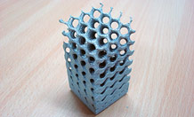 |
| A complex SLM part |
Producing strong, lightweight and complex parts for car manufacturing and the aerospace industry is set to become cheaper and more accurate thanks to a new technique developed by engineers from the University of Exeter. The research team has developed a new method for making three-dimensional aluminium composite parts by mixing a combination of relatively inexpensive powders.
Combining these elements causes a reaction which results in the production of particles that are 600 times smaller than the width of a human hair. Around 100 nanometres in size, the reaction uniformly distributes them through the material, making it very strong.
The process is based on the emerging technique of Selective Laser Manufacturing (SLM), in which laser manufactures complicated parts from metal powders, at the University’s Centre for Additive Layer Manufacturing. The new technique has the potential to manufacture aluminium composite parts as pistons, drive shafts, suspension components, brake discs and almost any structural components of cars or aeroplanes. It also enables the production of lighter structural designs with innovative geometries leading to further reduce of the weight of products.
The team’s latest research findings are published in the Journal of Alloys and Compounds.
Parts for cars and aeroplanes are widely made from aluminium, which is relatively light, with other reinforcement particles to make it stronger. The traditional methods, generally involved casting and mechanical alloying, can be inaccurate and expensive, especially when the part has a complex shape. Over the last decade, new SLM techniques have been developed, which enable parts with more complicated shapes to be produced. The new SLM techniques can be applied to manufacture aluminium composite parts from specific powder mixtures.
To carry out this new technique, the researchers use a laser to melt a mixture of powders, composed of aluminium and a reactive reinforcing material for example an iron oxide combination. A reaction between the powders results in the formation of new particles, which act as reinforcements and distribute evenly throughout the composite material.
This method allows parts with complex shapes to be easily produced. The new materials have very fine particles compared with other composites, making them more robust. The reaction between constituents releases energy, which also means materials can be produced at a higher rate using less power. This technique is significantly cheaper and more sustainable than other SLM methods which directly blend very fine powders to manufacture composites.
University of Exeter PhD student Sasan Dadbakhsh of the College of Engineering, Mathematics and Physical Sciences said: “This new development has great potential to make high performance parts for car manufacturing, the aerospace industry and potentially other industries. Additive layer manufacturing technologies are becoming increasingly accessible so this method could become a viable approach for manufacturing."
Dr Liang Hao of the University of Exeter added: “This advancement allows the rapid development of sustainable lightweight composite components. This particularly helps to save a considerable amount of material, energy and cost for the production of one-off or small volume products.”
The Centre for Additive Layer Manufacturing (CALM) is a £2.6 million investment in innovative manufacturing for the benefit of businesses in the South West and across the rest of the UK. CALM is delivered in collaboration with EADS UK Ltd.
Source: University of Exeter
Additional Information:
- Published in the Journal of Alloys and Compounds ("Effect of Al alloys on selective laser melting behaviour and microstructure of in-situ formed particle reinforced composites").
Lightening the load: new materials for automotive
The Engineer
July 2, 2012
Steel could one day be replaced as the material of choice for high-volume auto manufacture, but installed plant and entrenched manufacturing processes make the transition difficult
We’re in a brave new world of engineering innovation, with new inventions and developments enriching our lives every day. Yet some aspects of the devices we depend on have changed little from their inception. It might seem like a contradiction, but sometimes even the most innovative sectors find there are barriers to innovation.
Take, for example, the most visible example of the way technology changed our lives in the last century: the motor car. In many ways, the cars on the roads today are unrecognisable from the contraptions and the early fruits of mass production that trundled down the roads of the 1910s and 1920s. But in others, they have changed very little.
‘People have the perception that cars are basically steel boxes with glass windows, and there’s a good reason for that perception,’ said Prof Richard Dashwood, head of materials and sustainability at the Warwick Manufacturing Group (WMG) and chief technology officer of the new High Value Manufacturing Catapult centre. ‘It is because, largely, they are. Something like 99.9 per cent of all cars on the road are steel-intensive vehicles.’
But the issue of ‘lightweighting’ — reducing the mass of the vehicle — is very much on the minds of automotive manufacturers at the moment. ‘It’s driven by European legislation on CO2 emissions,’ Dashwood said. ‘While you can improve your powertrain and aerodynamics, it’s lightweighting that will give you the biggest CO2 improvement.’
So why, considering the many advances in materials that have taken place over the last century and which have been adopted so enthusiastically by, for example, the aerospace sector, is the automotive industry still so wedded to its original materials?
There are exceptions to this rule. Among the most notable is Jaguar Land Rover, which switched to all-aluminium bodies in 2009, after Jaguar led the way with aluminium construction with the XJ and XK models. Aluminium is, of course, lighter than steel with comparable strength. ‘We didn’t decide to use aluminium because it was new or different,’ said Jaguar’s chief technical specialist for body engineering, Mark White. ‘It is because aluminium delivers significant benefits for drivers.’
July 2, 2012
 |
In the automotive sector, mineral fillers such as glass fibre are being replaced by materials such as hemp
|
We’re in a brave new world of engineering innovation, with new inventions and developments enriching our lives every day. Yet some aspects of the devices we depend on have changed little from their inception. It might seem like a contradiction, but sometimes even the most innovative sectors find there are barriers to innovation.
Take, for example, the most visible example of the way technology changed our lives in the last century: the motor car. In many ways, the cars on the roads today are unrecognisable from the contraptions and the early fruits of mass production that trundled down the roads of the 1910s and 1920s. But in others, they have changed very little.
‘People have the perception that cars are basically steel boxes with glass windows, and there’s a good reason for that perception,’ said Prof Richard Dashwood, head of materials and sustainability at the Warwick Manufacturing Group (WMG) and chief technology officer of the new High Value Manufacturing Catapult centre. ‘It is because, largely, they are. Something like 99.9 per cent of all cars on the road are steel-intensive vehicles.’
But the issue of ‘lightweighting’ — reducing the mass of the vehicle — is very much on the minds of automotive manufacturers at the moment. ‘It’s driven by European legislation on CO2 emissions,’ Dashwood said. ‘While you can improve your powertrain and aerodynamics, it’s lightweighting that will give you the biggest CO2 improvement.’
So why, considering the many advances in materials that have taken place over the last century and which have been adopted so enthusiastically by, for example, the aerospace sector, is the automotive industry still so wedded to its original materials?
There are exceptions to this rule. Among the most notable is Jaguar Land Rover, which switched to all-aluminium bodies in 2009, after Jaguar led the way with aluminium construction with the XJ and XK models. Aluminium is, of course, lighter than steel with comparable strength. ‘We didn’t decide to use aluminium because it was new or different,’ said Jaguar’s chief technical specialist for body engineering, Mark White. ‘It is because aluminium delivers significant benefits for drivers.’
Northwestern Researchers Create “Rubber-Band Electronics”
Engineerblogger
July 2, 2012
For people with heart conditions and other ailments that require monitoring, life can be complicated by constant hospital visits and time-consuming tests. But what if much of the testing done at hospitals could be conducted in the patient’s home, office, or car?
Scientists foresee a time when medical monitoring devices are integrated seamlessly into the human body, able to track a patient’s vital signs and transmit them to his doctors. But one major obstacle continues to hinder technologies like these: electronics are too rigid.
Researchers at the McCormick School of Engineering, working with a team of scientists from the United States and abroad, have recently developed a design that allows electronics to bend and stretch to more than 200 percent their original size, four times greater than is possible with today’s technology. The key is a combination of a porous polymer and liquid metal.
A paper about the findings, “Three-dimensional Nanonetworks for Giant Stretchability in Dielectrics and Conductors,” was published June 26 in the journal Nature Communications.
“With current technology, electronics are able to stretch a small amount, but many potential applications require a device to stretch like a rubber band,” said Yonggang Huang, Joseph Cummings Professor of Civil and Environmental Engineering and Mechanical Engineering, who conducted the research with partners at the Korea Advanced Institute of Science and Technology (South Korea), Dalian University of Technology (China), and the University of Illinois at Urbana-Champaign. “With that level of stretchability we could see medical devices integrated into the human body.”
In the past five years, Huang and collaborators at the University of Illinois have developed electronics with about 50 percent stretchability, but this is not high enough for many applications.
One challenge facing these researchers has been overcoming a loss of conductivity in stretchable electronics. Circuits made from solid metals that are on the market today can survive a small amount of stretch, but their electrical conductivity plummets by 100 times when stretched. “This conductivity loss really defeats the point of stretchable electronics,” Huang said.
Huang’s team has found a way to overcome these challenges. First, they created a highly porous three-dimensional structure using a polymer material, poly(dimethylsiloxane) (PDMS), that can stretch to three times its original size. Then they placed a liquid metal (EGaIn) inside the pores, allowing electricity to flow consistently even when the material is excessively stretched.
The result is a material that is both highly stretchable and extremely conductive.
“By combining a liquid metal in a porous polymer, we achieved 200 percent stretchability in a material that does not suffer from stretch,” Huang said. “Once you achieve that technology, any electronic can behave like a rubber band.”
The graduate student Shuodao Wang at Northwestern University is a co-author of the paper.
Source: Northwestern University
July 2, 2012
 |
| Yonggang Huang |
For people with heart conditions and other ailments that require monitoring, life can be complicated by constant hospital visits and time-consuming tests. But what if much of the testing done at hospitals could be conducted in the patient’s home, office, or car?
Scientists foresee a time when medical monitoring devices are integrated seamlessly into the human body, able to track a patient’s vital signs and transmit them to his doctors. But one major obstacle continues to hinder technologies like these: electronics are too rigid.
Researchers at the McCormick School of Engineering, working with a team of scientists from the United States and abroad, have recently developed a design that allows electronics to bend and stretch to more than 200 percent their original size, four times greater than is possible with today’s technology. The key is a combination of a porous polymer and liquid metal.
A paper about the findings, “Three-dimensional Nanonetworks for Giant Stretchability in Dielectrics and Conductors,” was published June 26 in the journal Nature Communications.
“With current technology, electronics are able to stretch a small amount, but many potential applications require a device to stretch like a rubber band,” said Yonggang Huang, Joseph Cummings Professor of Civil and Environmental Engineering and Mechanical Engineering, who conducted the research with partners at the Korea Advanced Institute of Science and Technology (South Korea), Dalian University of Technology (China), and the University of Illinois at Urbana-Champaign. “With that level of stretchability we could see medical devices integrated into the human body.”
In the past five years, Huang and collaborators at the University of Illinois have developed electronics with about 50 percent stretchability, but this is not high enough for many applications.
One challenge facing these researchers has been overcoming a loss of conductivity in stretchable electronics. Circuits made from solid metals that are on the market today can survive a small amount of stretch, but their electrical conductivity plummets by 100 times when stretched. “This conductivity loss really defeats the point of stretchable electronics,” Huang said.
Huang’s team has found a way to overcome these challenges. First, they created a highly porous three-dimensional structure using a polymer material, poly(dimethylsiloxane) (PDMS), that can stretch to three times its original size. Then they placed a liquid metal (EGaIn) inside the pores, allowing electricity to flow consistently even when the material is excessively stretched.
The result is a material that is both highly stretchable and extremely conductive.
“By combining a liquid metal in a porous polymer, we achieved 200 percent stretchability in a material that does not suffer from stretch,” Huang said. “Once you achieve that technology, any electronic can behave like a rubber band.”
The graduate student Shuodao Wang at Northwestern University is a co-author of the paper.
Source: Northwestern University
Breakthrough could reduce costs for the consumer: Researchers' discovery to improve efficiencies in fuel, chemical and pharmaceutical industries
Engineerblogger
June 3, 2012
University of Minnesota engineering researchers are leading an international team that has made a major breakthrough in developing a catalyst used during chemical reactions in the production of gasoline, plastics, biofuels, pharmaceuticals, and other chemicals. The discovery could lead to major efficiencies and cost-savings in these multibillion-dollar industries.
The research is to be published in the June 29, 2012 issue of the leading scientific journal Science.
“The impact of this new discovery is enormous,” said the team’s lead researcher Michael Tsapatsis, a chemical engineering and materials science professor in the University of Minnesota College of Science and Engineering. “Every drop of gasoline we use needs a catalyst to change the oil molecules into usable gasoline during the refining process.”
This research improves efficiencies by giving molecules fast access to the catalysts where the chemical reactions occur. Tsapatsis compared it to our use of freeways and side streets in our daily lives.
“It’s faster and more efficient to use freeways to get where we want to go and exit to do our business compared to driving the side streets the entire way,” he explained. “The catalysts used today are more like all side streets. Molecules move slowly and get stuck. The efficiencies of these new catalysts could lower the costs of gasoline and other products for all of us.”
The research team built their prototype of the new catalyst using highly optimized ultra-thin zeolite nanosheets. They used a unique process to encourage growth of these nanosheets at 90-degree angles, similar to building a house of cards. The house-of-cards arrangement of the nanosheets makes the catalyst faster, more selective and more stable, but can be made at the same cost (or possibly cheaper) than traditional catalysts.
With faster catalysts available at no extra cost to the producer, production per manufacturing dollar will increase. With a higher output, it is conceivable that consumer costs will drop.
This new discovery builds upon previous discoveries at the University of Minnesota of ultra-thin zeolite nanosheets used as specialized molecular sieves for production of both renewable and fossil-based fuels and chemicals. These discoveries, licensed by the new Minnesota start-up company Argilex Technologies, are key components of the company’s materials-based platform. The development of the new catalyst is complete, and the material is ready for customer testing.
“This breakthrough can have a major impact on both the conversion of natural gas to higher value chemicals and fuels, and on bio- and petroleum refiners,” said Cesar Gonzalez, CEO of Argilex Technologies. “Using catalysts made by this novel approach, refiners will be able to obtain a higher yield of desirable products such as gasoline, diesel, ethylene and propylene. At Argilex, we envision this catalyst technology platform to become a key contributor to efficient use of natural resources and improved economics of the world’s largest industries.“
Researchers on the team are from around the globe. In addition to the University of Minnesota, researchers are from institutions in Tokyo, Abu Dhabi, Korea and Sweden.
Primary funding for this research is from the U.S. Department of Energy’s Center for Catalysis and Energy Innovation, an Energy Frontier Research Center. The University of Minnesota is a partner in this multi-institutional research center at the University of Delaware. Other funding for this research is from the National Science Foundation Emerging Frontiers in Research and Innovation Program, the University of Minnesota’s Initiative for Renewable Energy and the Environment, and the Abu Dhabi-Minnesota Institute for Research Excellence (ADMIRE) partnership between the University of Minnesota and the Abu Dhabi Petroleum Institute.
Read the full research paper entitled “Synthesis of Self-Pillared Zeolite Nanosheets by Repetitive Branching,” on the Science website: http://z.umn.edu/catalyst.
Source: University of Minnesota
June 3, 2012
 |
| The research team built their prototype of the new catalyst using ultra-thin zeolite nanosheets. They used a unique process to encourage growth of these nanosheets at 90-degree angles, similar to building a house of cards. |
University of Minnesota engineering researchers are leading an international team that has made a major breakthrough in developing a catalyst used during chemical reactions in the production of gasoline, plastics, biofuels, pharmaceuticals, and other chemicals. The discovery could lead to major efficiencies and cost-savings in these multibillion-dollar industries.
The research is to be published in the June 29, 2012 issue of the leading scientific journal Science.
“The impact of this new discovery is enormous,” said the team’s lead researcher Michael Tsapatsis, a chemical engineering and materials science professor in the University of Minnesota College of Science and Engineering. “Every drop of gasoline we use needs a catalyst to change the oil molecules into usable gasoline during the refining process.”
This research improves efficiencies by giving molecules fast access to the catalysts where the chemical reactions occur. Tsapatsis compared it to our use of freeways and side streets in our daily lives.
“It’s faster and more efficient to use freeways to get where we want to go and exit to do our business compared to driving the side streets the entire way,” he explained. “The catalysts used today are more like all side streets. Molecules move slowly and get stuck. The efficiencies of these new catalysts could lower the costs of gasoline and other products for all of us.”
The research team built their prototype of the new catalyst using highly optimized ultra-thin zeolite nanosheets. They used a unique process to encourage growth of these nanosheets at 90-degree angles, similar to building a house of cards. The house-of-cards arrangement of the nanosheets makes the catalyst faster, more selective and more stable, but can be made at the same cost (or possibly cheaper) than traditional catalysts.
With faster catalysts available at no extra cost to the producer, production per manufacturing dollar will increase. With a higher output, it is conceivable that consumer costs will drop.
This new discovery builds upon previous discoveries at the University of Minnesota of ultra-thin zeolite nanosheets used as specialized molecular sieves for production of both renewable and fossil-based fuels and chemicals. These discoveries, licensed by the new Minnesota start-up company Argilex Technologies, are key components of the company’s materials-based platform. The development of the new catalyst is complete, and the material is ready for customer testing.
“This breakthrough can have a major impact on both the conversion of natural gas to higher value chemicals and fuels, and on bio- and petroleum refiners,” said Cesar Gonzalez, CEO of Argilex Technologies. “Using catalysts made by this novel approach, refiners will be able to obtain a higher yield of desirable products such as gasoline, diesel, ethylene and propylene. At Argilex, we envision this catalyst technology platform to become a key contributor to efficient use of natural resources and improved economics of the world’s largest industries.“
Researchers on the team are from around the globe. In addition to the University of Minnesota, researchers are from institutions in Tokyo, Abu Dhabi, Korea and Sweden.
Primary funding for this research is from the U.S. Department of Energy’s Center for Catalysis and Energy Innovation, an Energy Frontier Research Center. The University of Minnesota is a partner in this multi-institutional research center at the University of Delaware. Other funding for this research is from the National Science Foundation Emerging Frontiers in Research and Innovation Program, the University of Minnesota’s Initiative for Renewable Energy and the Environment, and the Abu Dhabi-Minnesota Institute for Research Excellence (ADMIRE) partnership between the University of Minnesota and the Abu Dhabi Petroleum Institute.
Read the full research paper entitled “Synthesis of Self-Pillared Zeolite Nanosheets by Repetitive Branching,” on the Science website: http://z.umn.edu/catalyst.
Source: University of Minnesota
Subscribe to:
Posts (Atom)