
Engineerblogger
Feb 18, 2013
Paved roads are nice to look at, but they’re easily damaged and costly to repair. Erik Schlangen demos a new type of porous asphalt made of simple materials with an astonishing feature: When cracked, it can be “healed” by induction heating.
Source: TED
Additional Information:
Showing posts with label Materials. Show all posts
Showing posts with label Materials. Show all posts
Monday, 18 February 2013
Friday, 15 February 2013
New carbon films improve prospects of solar energy devices
Engineerblogger
Feb 15, 2013
New research by Yale University scientists helps pave the way for the next generation of solar cells, a renewable energy technology that directly converts solar energy into electricity.
In a pair of recent papers, Yale engineers report a novel and cost-effective way to improve the efficiency of crystalline silicon solar cells through the application of thin, smooth carbon nanotube films. These films could be used to produce hybrid carbon/silicon solar cells with far greater power-conversion efficiency than reported in this system to date.
“Our approach bridges the cost-effectiveness and excellent electrical and optical properties of novel nanomaterials with well-established, high efficiency silicon solar cell technologies,” said André D. Taylor, assistant professor of chemical and environmental engineering at Yale and a principal investigator of the research.
The researchers reported their work in two papers published in December, one in the journal Energy and Environmental Science and one in Nano Letters (Record High Efficiency Single-Walled Carbon Nanotube/Silicon p–n Junction Solar Cells). Mark A. Reed, a professor of electrical engineering and applied physics at Yale, is also a principal investigator.
Silicon, an abundant element, is an ideal material for solar cells because its optical properties make it an intrinsically efficient energy converter. But the high cost of processing single-crystalline silicon at necessarily high temperatures has hindered widespread commercialization.
Organic solar cells — an existing alternative to high-cost crystalline silicon solar cells — allow for simpler, room-temperature processing and lower costs, researchers said, but they have low power-conversion efficiency.
Instead of using only organic substitutes, the Yale team applied thin, smooth carbon nanotube films with superior conductance and optical properties to the surface of single crystalline silicon to create a hybrid solar cell architecture. To do it, they developed a method called superacid sliding.
As reported in the papers, the approach allows them to take advantage of the desirable photovoltaic properties of single-crystalline silicon through a simpler, low-temperature, lower-cost process. It allows for both high light absorption and high electrical conductivity.
“This is striking, as it suggests that the superior photovoltaic properties of single-crystalline silicon can be realized by a simple, low-temperature process,” said Xiaokai Li, a doctoral student in Taylor’s lab and a lead author on both papers. “The secret lies in the arrangement and assembly of these carbon nanotube thin films,”
In previous work, Yale scientist successfully developed a carbon nanotube composite thin film that could be used in fuel cells and lithium ion batteries. The recent research suggests how to extend the film’s application to solar cells by optimizing its smoothness and durability.
“Optimizing this interface could also serve as a platform for many next-generation solar cell devices, including carbon nanotube/polymer, carbon/polymer, and all carbon solar cells,” said Yeonwoong (Eric) Jung, a postdoctoral researcher in Reed’s lab and also a lead author of the papers.
All authors are listed on the papers (links above).
The National Science Foundation, NASA, the U.S. Department of Energy, and the Yale Institute for Nanoscience and Quantum Engineering provided support for the research.
Source: Yale University
Additional Information:
Feb 15, 2013
 |
| New research by Yale University scientists helps pave the way for the next generation of solar cells, a renewable energy technology that directly converts solar energy into electricity. (Illustration by the researchers) |
New research by Yale University scientists helps pave the way for the next generation of solar cells, a renewable energy technology that directly converts solar energy into electricity.
In a pair of recent papers, Yale engineers report a novel and cost-effective way to improve the efficiency of crystalline silicon solar cells through the application of thin, smooth carbon nanotube films. These films could be used to produce hybrid carbon/silicon solar cells with far greater power-conversion efficiency than reported in this system to date.
“Our approach bridges the cost-effectiveness and excellent electrical and optical properties of novel nanomaterials with well-established, high efficiency silicon solar cell technologies,” said André D. Taylor, assistant professor of chemical and environmental engineering at Yale and a principal investigator of the research.
The researchers reported their work in two papers published in December, one in the journal Energy and Environmental Science and one in Nano Letters (Record High Efficiency Single-Walled Carbon Nanotube/Silicon p–n Junction Solar Cells). Mark A. Reed, a professor of electrical engineering and applied physics at Yale, is also a principal investigator.
Silicon, an abundant element, is an ideal material for solar cells because its optical properties make it an intrinsically efficient energy converter. But the high cost of processing single-crystalline silicon at necessarily high temperatures has hindered widespread commercialization.
Organic solar cells — an existing alternative to high-cost crystalline silicon solar cells — allow for simpler, room-temperature processing and lower costs, researchers said, but they have low power-conversion efficiency.
Instead of using only organic substitutes, the Yale team applied thin, smooth carbon nanotube films with superior conductance and optical properties to the surface of single crystalline silicon to create a hybrid solar cell architecture. To do it, they developed a method called superacid sliding.
As reported in the papers, the approach allows them to take advantage of the desirable photovoltaic properties of single-crystalline silicon through a simpler, low-temperature, lower-cost process. It allows for both high light absorption and high electrical conductivity.
“This is striking, as it suggests that the superior photovoltaic properties of single-crystalline silicon can be realized by a simple, low-temperature process,” said Xiaokai Li, a doctoral student in Taylor’s lab and a lead author on both papers. “The secret lies in the arrangement and assembly of these carbon nanotube thin films,”
In previous work, Yale scientist successfully developed a carbon nanotube composite thin film that could be used in fuel cells and lithium ion batteries. The recent research suggests how to extend the film’s application to solar cells by optimizing its smoothness and durability.
“Optimizing this interface could also serve as a platform for many next-generation solar cell devices, including carbon nanotube/polymer, carbon/polymer, and all carbon solar cells,” said Yeonwoong (Eric) Jung, a postdoctoral researcher in Reed’s lab and also a lead author of the papers.
All authors are listed on the papers (links above).
The National Science Foundation, NASA, the U.S. Department of Energy, and the Yale Institute for Nanoscience and Quantum Engineering provided support for the research.
Source: Yale University
Additional Information:
Forget about leprechauns, engineers are catching rainbows
Engineerblogger
Feb 15, 2012
University at Buffalo engineers have created a more efficient way to catch rainbows, an advancement in photonics that could lead to technological breakthroughs in solar energy, stealth technology and other areas of research.
Qiaoqiang Gan, PhD, an assistant professor of electrical engineering at UB, and a team of graduate students described their work in a paper called “Rainbow Trapping in Hyperbolic Metamaterial Waveguide,” published in the online journal Scientific Reports.
They developed a “hyperbolic metamaterial waveguide,” which is essentially an advanced microchip made of alternate ultra-thin films of metal and semiconductors and/or insulators. The waveguide halts and ultimately absorbs each frequency of light, at slightly different places in a vertical direction (see the above figure), to catch a “rainbow” of wavelengths.
Gan is a researcher within UB’s new Center of Excellence in Materials Informatics.
“Electromagnetic absorbers have been studied for many years, especially for military radar systems,” Gan said. “Right now, researchers are developing compact light absorbers based on optically thick semiconductors or carbon nanotubes. However, it is still challenging to realize the perfect absorber in ultra-thin films with tunable absorption band.
“We are developing ultra-thin films that will slow the light and therefore allow much more efficient absorption, which will address the long existing challenge.”
Light is made of photons that, because they move extremely fast (i.e., at the speed of light), are difficult to tame. In their initial attempts to slow light, researchers relied upon cryogenic gases. But because cryogenic gases are very cold – roughly 240 degrees below zero Fahrenheit – they are difficult to work with outside a laboratory.
Before joining UB, Gan helped pioneer a way to slow light without cryogenic gases. He and other researchers at Lehigh University made nano-scale-sized grooves in metallic surfaces at different depths, a process that altered the optical properties of the metal. While the grooves worked, they had limitations. For example, the energy of the incident light cannot be transferred onto the metal surface efficiently, which hampered its use for practical applications, Gan said.
The hyperbolic metamaterial waveguide solves that problem because it is a large area of patterned film that can collect the incident light efficiently. It is referred to as an artificial medium with subwavelength features whose frequency surface is hyperboloid, which allows it to capture a wide range of wavelengths in different frequencies including visible, near-infrared, mid-infrared, terahertz and microwaves.
It could lead to advancements in an array of fields.
For example, in electronics there is a phenomenon known as crosstalk, in which a signal transmitted on one circuit or channel creates an undesired effect in another circuit or channel. The on-chip absorber could potentially prevent this.
The on-chip absorber may also be applied to solar panels and other energy-harvesting devices. It could be especially useful in mid-infrared spectral regions as thermal absorber for devices that recycle heat after sundown, Gan said.
Technology such as the Stealth bomber involves materials that make planes, ships and other devices invisible to radar, infrared, sonar and other detection methods. Because the on-chip absorber has the potential to absorb different wavelengths at a multitude of frequencies, it could be useful as a stealth coating material.
Additional authors of the paper include Haifeng Hu, Dengxin Ji, Xie Zeng and Kai Liu, all PhD candidates in UB’s Department of Electrical Engineering. The work was sponsored by the National Science Foundation and UB’s electrical engineering department.
Source: University of Buffalo
Additional Information:
Related Article:
Feb 15, 2012
 |
| An up-close look at the “hyperbolic metamaterial waveguide,” which catches and ultimately absorbs wavelengths (or color) in a vertical direction. |
University at Buffalo engineers have created a more efficient way to catch rainbows, an advancement in photonics that could lead to technological breakthroughs in solar energy, stealth technology and other areas of research.
Qiaoqiang Gan, PhD, an assistant professor of electrical engineering at UB, and a team of graduate students described their work in a paper called “Rainbow Trapping in Hyperbolic Metamaterial Waveguide,” published in the online journal Scientific Reports.
They developed a “hyperbolic metamaterial waveguide,” which is essentially an advanced microchip made of alternate ultra-thin films of metal and semiconductors and/or insulators. The waveguide halts and ultimately absorbs each frequency of light, at slightly different places in a vertical direction (see the above figure), to catch a “rainbow” of wavelengths.
Gan is a researcher within UB’s new Center of Excellence in Materials Informatics.
“Electromagnetic absorbers have been studied for many years, especially for military radar systems,” Gan said. “Right now, researchers are developing compact light absorbers based on optically thick semiconductors or carbon nanotubes. However, it is still challenging to realize the perfect absorber in ultra-thin films with tunable absorption band.
“We are developing ultra-thin films that will slow the light and therefore allow much more efficient absorption, which will address the long existing challenge.”
Light is made of photons that, because they move extremely fast (i.e., at the speed of light), are difficult to tame. In their initial attempts to slow light, researchers relied upon cryogenic gases. But because cryogenic gases are very cold – roughly 240 degrees below zero Fahrenheit – they are difficult to work with outside a laboratory.
Before joining UB, Gan helped pioneer a way to slow light without cryogenic gases. He and other researchers at Lehigh University made nano-scale-sized grooves in metallic surfaces at different depths, a process that altered the optical properties of the metal. While the grooves worked, they had limitations. For example, the energy of the incident light cannot be transferred onto the metal surface efficiently, which hampered its use for practical applications, Gan said.
The hyperbolic metamaterial waveguide solves that problem because it is a large area of patterned film that can collect the incident light efficiently. It is referred to as an artificial medium with subwavelength features whose frequency surface is hyperboloid, which allows it to capture a wide range of wavelengths in different frequencies including visible, near-infrared, mid-infrared, terahertz and microwaves.
It could lead to advancements in an array of fields.
For example, in electronics there is a phenomenon known as crosstalk, in which a signal transmitted on one circuit or channel creates an undesired effect in another circuit or channel. The on-chip absorber could potentially prevent this.
The on-chip absorber may also be applied to solar panels and other energy-harvesting devices. It could be especially useful in mid-infrared spectral regions as thermal absorber for devices that recycle heat after sundown, Gan said.
Technology such as the Stealth bomber involves materials that make planes, ships and other devices invisible to radar, infrared, sonar and other detection methods. Because the on-chip absorber has the potential to absorb different wavelengths at a multitude of frequencies, it could be useful as a stealth coating material.
Additional authors of the paper include Haifeng Hu, Dengxin Ji, Xie Zeng and Kai Liu, all PhD candidates in UB’s Department of Electrical Engineering. The work was sponsored by the National Science Foundation and UB’s electrical engineering department.
Source: University of Buffalo
Additional Information:
Related Article:
Tuesday, 12 February 2013
Stem cell breakthrough could lead to new bone repair therapies on nanoscale surfaces
Engineerblogger
Feb 12, 2013
Scientists at the University of Southampton have created a new method to generate bone cells which could lead to revolutionary bone repair therapies for people with bone fractures or those who need hip replacement surgery due to osteoporosis and osteoarthritis.
The research, carried out by Dr Emmajayne Kingham at the University of Southampton in collaboration with the University of Glasgow and published in the journal Small, cultured human embryonic stem cells on to the surface of plastic materials and assessed their ability to change.
Scientists were able to use the nanotopographical patterns on the biomedical plastic to manipulate human embryonic stem cells towards bone cells. This was done without any chemical enhancement.
The materials, including the biomedical implantable material polycarbonate plastic, which is a versatile plastic used in things from bullet proof windows to CDs, offer an accessible and cheaper way of culturing human embryonic stem cells and presents new opportunities for future medical research in this area.
Professor Richard Oreffo, who led the University of Southampton team, explains: “To generate bone cells for regenerative medicine and further medical research remains a significant challenge. However we have found that by harnessing surface technologies that allow the generation and ultimately scale up of human embryonic stem cells to skeletal cells, we can aid the tissue engineering process. This is very exciting.
“Our research may offer a whole new approach to skeletal regenerative medicine. The use of nanotopographical patterns could enable new cell culture designs, new device designs, and could herald the development of new bone repair therapies as well as further human stem cell research,” Professor Oreffo adds.
The study was funded by the Biotechnology and Biological Sciences Research Council (BBSRC).
This latest discovery expands on the close collaborative work previously undertaken by the University of Southampton and the University of Glasgow. In 2011 the team successfully used plastic with embossed nanopatterns to grow and spread adult stem cells while keeping their stem cell characteristics; a process which is cheaper and easier to manufacture than previous ways of working.
Dr Nikolaj Gadegaard, Institute of Molecular, Cell and Systems Biology at the University of Glasgow, says: "Our previous collaborative research showed exciting new ways to control mesenchymal stem cell – stem cells from the bone marrow of adults – growth and differentiation on nanoscale patterns.
“This new Southampton-led discovery shows a totally different stem cell source, embryonic, also respond in a similar manner and this really starts to open this new field of discovery up. With more research impetus, it gives us the hope that we can go on to target a wider variety of degenerative conditions than we originally aspired to. This result is of fundamental significance."
Source: University of Southampton
Feb 12, 2013
 |
| Stem cell breakthrough could lead to new bone repair therapies |
Scientists at the University of Southampton have created a new method to generate bone cells which could lead to revolutionary bone repair therapies for people with bone fractures or those who need hip replacement surgery due to osteoporosis and osteoarthritis.
The research, carried out by Dr Emmajayne Kingham at the University of Southampton in collaboration with the University of Glasgow and published in the journal Small, cultured human embryonic stem cells on to the surface of plastic materials and assessed their ability to change.
Scientists were able to use the nanotopographical patterns on the biomedical plastic to manipulate human embryonic stem cells towards bone cells. This was done without any chemical enhancement.
The materials, including the biomedical implantable material polycarbonate plastic, which is a versatile plastic used in things from bullet proof windows to CDs, offer an accessible and cheaper way of culturing human embryonic stem cells and presents new opportunities for future medical research in this area.
Professor Richard Oreffo, who led the University of Southampton team, explains: “To generate bone cells for regenerative medicine and further medical research remains a significant challenge. However we have found that by harnessing surface technologies that allow the generation and ultimately scale up of human embryonic stem cells to skeletal cells, we can aid the tissue engineering process. This is very exciting.
“Our research may offer a whole new approach to skeletal regenerative medicine. The use of nanotopographical patterns could enable new cell culture designs, new device designs, and could herald the development of new bone repair therapies as well as further human stem cell research,” Professor Oreffo adds.
The study was funded by the Biotechnology and Biological Sciences Research Council (BBSRC).
This latest discovery expands on the close collaborative work previously undertaken by the University of Southampton and the University of Glasgow. In 2011 the team successfully used plastic with embossed nanopatterns to grow and spread adult stem cells while keeping their stem cell characteristics; a process which is cheaper and easier to manufacture than previous ways of working.
Dr Nikolaj Gadegaard, Institute of Molecular, Cell and Systems Biology at the University of Glasgow, says: "Our previous collaborative research showed exciting new ways to control mesenchymal stem cell – stem cells from the bone marrow of adults – growth and differentiation on nanoscale patterns.
“This new Southampton-led discovery shows a totally different stem cell source, embryonic, also respond in a similar manner and this really starts to open this new field of discovery up. With more research impetus, it gives us the hope that we can go on to target a wider variety of degenerative conditions than we originally aspired to. This result is of fundamental significance."
Source: University of Southampton
Monday, 11 February 2013
Implants make light work of fixing broken bones
Engineerblogger
Feb 11, 2013
Artificial bone, created using stem cells and a new lightweight plastic, could soon be used to heal shattered limbs.
The use of bone stem cells combined with a degradable rigid material that inserts into broken bones and encourages real bone to re-grow has been developed at the Universities of Edinburgh and Southampton.
Researchers have developed the material with a honeycomb scaffold structure that allows blood to flow through it, enabling stem cells from the patient’s bone marrow to attach to the material and grow new bone. Over time, the plastic slowly degrades as the implant is replaced by newly grown bone.
Scientists developed the material by blending three types of plastics. They used a pioneering technique to blend and test hundreds of combinations of plastics, to identify a blend that was robust, lightweight, and able to support bone stem cells. Successful results have been shown in the lab and in animal testing with the focus now moving towards human clinical evaluation.
The study, published in the journal Advanced Functional Materials, was funded by the Biotechnology and Biological Sciences Research Council.
This new discovery is the result of a seven-year partnership between the University of Southampton and the University of Edinburgh.
Richard Oreffo, Professor of Musculoskeletal Science at the University of Southampton, comments: "Fractures and bone loss due to trauma or disease are a significant clinical and socioeconomic problem. This collaboration between chemistry and medicine has identified unique candidate materials that support human bone stem cell growth and allow bone formation. Our collaborative strategy offers significant therapeutic implications."
Professor Mark Bradley, of the University of Edinburgh’s School of Chemistry, adds: “We were able to make and look at a hundreds of candidate materials and rapidly whittle these down to one which is strong enough to replace bone and is also a suitable surface upon which to grow new bone.
“We are confident that this material could soon be helping to improve the quality of life for patients with severe bone injuries, and will help maintain the health of an ageing population.”
Source: University of Southampton
Feb 11, 2013
 |
| Richard Oreffo |
Artificial bone, created using stem cells and a new lightweight plastic, could soon be used to heal shattered limbs.
The use of bone stem cells combined with a degradable rigid material that inserts into broken bones and encourages real bone to re-grow has been developed at the Universities of Edinburgh and Southampton.
Researchers have developed the material with a honeycomb scaffold structure that allows blood to flow through it, enabling stem cells from the patient’s bone marrow to attach to the material and grow new bone. Over time, the plastic slowly degrades as the implant is replaced by newly grown bone.
Scientists developed the material by blending three types of plastics. They used a pioneering technique to blend and test hundreds of combinations of plastics, to identify a blend that was robust, lightweight, and able to support bone stem cells. Successful results have been shown in the lab and in animal testing with the focus now moving towards human clinical evaluation.
The study, published in the journal Advanced Functional Materials, was funded by the Biotechnology and Biological Sciences Research Council.
This new discovery is the result of a seven-year partnership between the University of Southampton and the University of Edinburgh.
Richard Oreffo, Professor of Musculoskeletal Science at the University of Southampton, comments: "Fractures and bone loss due to trauma or disease are a significant clinical and socioeconomic problem. This collaboration between chemistry and medicine has identified unique candidate materials that support human bone stem cell growth and allow bone formation. Our collaborative strategy offers significant therapeutic implications."
Professor Mark Bradley, of the University of Edinburgh’s School of Chemistry, adds: “We were able to make and look at a hundreds of candidate materials and rapidly whittle these down to one which is strong enough to replace bone and is also a suitable surface upon which to grow new bone.
“We are confident that this material could soon be helping to improve the quality of life for patients with severe bone injuries, and will help maintain the health of an ageing population.”
Source: University of Southampton
Saturday, 12 January 2013
How to treat heat like light: Using nanoparticle alloys allows heat to be focused or reflected just like electromagnetic waves
Engineerblogger
Jan 12, 2012
An MIT researcher has developed a technique that provides a new way of manipulating heat, allowing it to be controlled much as light waves can be manipulated by lenses and mirrors.
The approach relies on engineered materials consisting of nanostructured semiconductor alloy crystals. Heat is a vibration of matter — technically, a vibration of the atomic lattice of a material — just as sound is. Such vibrations can also be thought of as a stream of phonons — a kind of “virtual particle” that is analogous to the photons that carry light. The new approach is similar to recently developed photonic crystals that can control the passage of light, and phononic crystals that can do the same for sound.
The spacing of tiny gaps in these materials is tuned to match the wavelength of the heat phonons, explains Martin Maldovan, a research scientist in MIT’s Department of Materials Science and Engineering and author of a paper on the new findings published Jan. 11 in the journal Physical Review Letters.
“It’s a completely new way to manipulate heat,” Maldovan says. Heat differs from sound, he explains, in the frequency of its vibrations: Sound waves consist of lower frequencies (up to the kilohertz range, or thousands of vibrations per second), while heat arises from higher frequencies (in the terahertz range, or trillions of vibrations per second).
In order to apply the techniques already developed to manipulate sound, Maldovan’s first step was to reduce the frequency of the heat phonons, bringing it closer to the sound range. He describes this as “hypersonic heat.”
“Phonons for sound can travel for kilometers,” Maldovan says — which is why it’s possible to hear noises from very far away. “But phonons of heat only travel for nanometers [billionths of a meter]. That’s why you couldn’t hear heat even with ears responding to terahertz frequencies.”
Heat also spans a wide range of frequencies, he says, while sound spans a single frequency. So, to address that, Maldovan says, “the first thing we did is reduce the number of frequencies of heat, and we made them lower,” bringing these frequencies down into the boundary zone between heat and sound. Making alloys of silicon that incorporate nanoparticles of germanium in a particular size range accomplished this lowering of frequency, he says.
Reducing the range of frequencies was also accomplished by making a series of thin films of the material, so that scattering of phonons would take place at the boundaries. This ends up concentrating most of the heat phonons within a relatively narrow “window” of frequencies.
Following the application of these techniques, more than 40 percent of the total heat flow is concentrated within a hypersonic range of 100 to 300 gigahertz, and most of the phonons align in a narrow beam, instead of moving in every direction.
As a result, this beam of narrow-frequency phonons can be manipulated using phononic crystals similar to those developed to control sound phonons. Because these crystals are now being used to control heat instead, Maldovan refers to them as “thermocrystals,” a new category of materials.
These thermocrystals might have a wide range of applications, he suggests, including in improved thermoelectric devices, which convert differences of temperature into electricity. Such devices transmit electricity freely while strictly controlling the flow of heat — tasks that the thermocrystals could accomplish very effectively, Maldovan says.
Most conventional materials allow heat to travel in all directions, like ripples expanding outward from a pebble dropped in a pond; thermocrystals could instead produce the equivalent of those ripples only moving out in a single direction, Maldovan says. The crystals could also be used to create thermal diodes: materials in which heat can pass in one direction, but not in the reverse direction. Such a one-way heat flow could be useful in energy-efficient buildings in hot and cold climates.
Other variations of the material could be used to focus heat — much like focusing light with a lens — to concentrate it in a small area. Another intriguing possibility is thermal cloaking, Maldovan says: materials that prevent detection of heat, just as recently developed metamaterials can create “invisibility cloaks” to shield objects from detection by visible light or microwaves.
Rama Venkatasubramanian, senior research director at the Center for Solid State Energetics at RTI International in North Carolina, says this is “an interesting approach to control the various frequencies of the phonon spectra that conduct heat in a solid-state material.”
The modeling used to develop this new system “needs to be further developed,” Venkatasubramanian adds. “The theory of what wavelengths of phonons, and at what temperatures, contribute to how much heat transport is a complex problem even in simpler materials, let alone nanostructured materials, and these will have to be factored in — so this paper will trigger more interest and study in that direction.”
Source: MIT
Jan 12, 2012
 |
| Thermal lattices, shown here, are one possible application of the newly developed thermocrystals. In these structures, where precisely spaced air gaps (dark circles) control the flow of heat, thermal energy can be "pinned" in place by defects introduced into the structure (colored areas). Illustration courtesy of Martin Maldovan |
An MIT researcher has developed a technique that provides a new way of manipulating heat, allowing it to be controlled much as light waves can be manipulated by lenses and mirrors.
The approach relies on engineered materials consisting of nanostructured semiconductor alloy crystals. Heat is a vibration of matter — technically, a vibration of the atomic lattice of a material — just as sound is. Such vibrations can also be thought of as a stream of phonons — a kind of “virtual particle” that is analogous to the photons that carry light. The new approach is similar to recently developed photonic crystals that can control the passage of light, and phononic crystals that can do the same for sound.
The spacing of tiny gaps in these materials is tuned to match the wavelength of the heat phonons, explains Martin Maldovan, a research scientist in MIT’s Department of Materials Science and Engineering and author of a paper on the new findings published Jan. 11 in the journal Physical Review Letters.
“It’s a completely new way to manipulate heat,” Maldovan says. Heat differs from sound, he explains, in the frequency of its vibrations: Sound waves consist of lower frequencies (up to the kilohertz range, or thousands of vibrations per second), while heat arises from higher frequencies (in the terahertz range, or trillions of vibrations per second).
In order to apply the techniques already developed to manipulate sound, Maldovan’s first step was to reduce the frequency of the heat phonons, bringing it closer to the sound range. He describes this as “hypersonic heat.”
“Phonons for sound can travel for kilometers,” Maldovan says — which is why it’s possible to hear noises from very far away. “But phonons of heat only travel for nanometers [billionths of a meter]. That’s why you couldn’t hear heat even with ears responding to terahertz frequencies.”
Heat also spans a wide range of frequencies, he says, while sound spans a single frequency. So, to address that, Maldovan says, “the first thing we did is reduce the number of frequencies of heat, and we made them lower,” bringing these frequencies down into the boundary zone between heat and sound. Making alloys of silicon that incorporate nanoparticles of germanium in a particular size range accomplished this lowering of frequency, he says.
Reducing the range of frequencies was also accomplished by making a series of thin films of the material, so that scattering of phonons would take place at the boundaries. This ends up concentrating most of the heat phonons within a relatively narrow “window” of frequencies.
Following the application of these techniques, more than 40 percent of the total heat flow is concentrated within a hypersonic range of 100 to 300 gigahertz, and most of the phonons align in a narrow beam, instead of moving in every direction.
As a result, this beam of narrow-frequency phonons can be manipulated using phononic crystals similar to those developed to control sound phonons. Because these crystals are now being used to control heat instead, Maldovan refers to them as “thermocrystals,” a new category of materials.
These thermocrystals might have a wide range of applications, he suggests, including in improved thermoelectric devices, which convert differences of temperature into electricity. Such devices transmit electricity freely while strictly controlling the flow of heat — tasks that the thermocrystals could accomplish very effectively, Maldovan says.
Most conventional materials allow heat to travel in all directions, like ripples expanding outward from a pebble dropped in a pond; thermocrystals could instead produce the equivalent of those ripples only moving out in a single direction, Maldovan says. The crystals could also be used to create thermal diodes: materials in which heat can pass in one direction, but not in the reverse direction. Such a one-way heat flow could be useful in energy-efficient buildings in hot and cold climates.
Other variations of the material could be used to focus heat — much like focusing light with a lens — to concentrate it in a small area. Another intriguing possibility is thermal cloaking, Maldovan says: materials that prevent detection of heat, just as recently developed metamaterials can create “invisibility cloaks” to shield objects from detection by visible light or microwaves.
Rama Venkatasubramanian, senior research director at the Center for Solid State Energetics at RTI International in North Carolina, says this is “an interesting approach to control the various frequencies of the phonon spectra that conduct heat in a solid-state material.”
The modeling used to develop this new system “needs to be further developed,” Venkatasubramanian adds. “The theory of what wavelengths of phonons, and at what temperatures, contribute to how much heat transport is a complex problem even in simpler materials, let alone nanostructured materials, and these will have to be factored in — so this paper will trigger more interest and study in that direction.”
Source: MIT
Saturday, 5 January 2013
Jumping droplets help heat transfer
Engineerblogger
Jan 4, 2013

Many industrial plants depend on water vapor condensing on metal plates: In power plants, the resulting water is then returned to a boiler to be vaporized again; in desalination plants, it yields a supply of clean water. The efficiency of such plants depends crucially on how easily droplets of water can form on these metal plates, or condensers, and how easily they fall away, leaving room for more droplets to form.
The key to improving the efficiency of such plants is to increase the condensers’ heat-transfer coefficient — a measure of how readily heat can be transferred away from those surfaces, explains Nenad Miljkovic, a doctoral student in mechanical engineering at MIT. As part of his thesis research, he and colleagues have done just that: designing, making and testing a coated surface with nanostructured patterns that greatly increase the heat-transfer coefficient.
The results of that work have been published in the journal Nano Letters, in a paper co-authored by Miljkovic, mechanical engineering associate professor Evelyn Wang, and five other researchers from the Device Research Lab (DRL) in MIT’s mechanical engineering department.
On a typical, flat-plate condenser, water vapor condenses to form a liquid film on the surface, drastically reducing the condenser’s ability to collect more water until gravity drains the film. “It acts as a barrier to heat transfer,” Miljkovic says. He and other researchers have focused on ways of encouraging water to bead up into droplets that then fall away from the surface, allowing more rapid water removal.
“The way to remove the thermal barrier is to remove [the droplets] as quickly as possible,” he says. Many researchers have studied ways of doing this by creating hydrophobic surfaces, either through chemical treatment or through surface patterning. But Miljkovic and his colleagues have now taken this a step further by making scalable surfaces with nanoscale features that barely touch the droplets.
The result: Droplets don’t just fall from the surface, but actually jump away from it, increasing the efficiency of the process. The energy released as tiny droplets merge to form larger ones is enough to propel the droplets upward from the surface, meaning the removal of droplets doesn’t depend solely on gravity.
Other researchers have worked on nanopatterned surfaces to induce such jumping, but these have tended to be complex and expensive to manufacture, usually requiring a clean-room environment. Those approaches also require flat surfaces, not the tubing or other shapes often used in condensers. Finally, prior research has not tested the enhanced heat transfer predicted for these types of surfaces.
In a paper published early in 2012, the MIT researchers showed that droplet shape is important to enhanced heat transfer. “Now, we’ve gone a step further,” Miljkovic says, “developing a surface that favors these kinds of droplets, while being highly scalable and easy to manufacture. Furthermore, we’ve actually been able to experimentally measure the heat-transfer enhancement.”
The patterning is done, Miljkovic says, using a simple wet-oxidation process right on the surface that can be applied to the copper tubes and plates commonly used in commercial power plants.
The nanostructured pattern itself is made of copper oxide and actually forms on top of the copper tubing. The process produces a surface that resembles a bed of tiny, pointed leaves sticking up from the surface; these nanoscale points minimize contact between the droplets and the surface, making release easier.
Not only can the nanostructured patterns be made and applied under room-temperature conditions, but the growth process naturally stops itself. “It’s a self-limiting reaction,” Miljkovic says, “whether you put it in [the treatment solution] for two minutes or two hours.”
After the leaflike pattern is created, a hydrophobic coating is applied when a vapor solution bonds itself to the patterned surface without significantly altering its shape. The team’s experiments showed that the efficiency of heat transfer using these treated surfaces could be increased by 30 percent, compared to today’s best hydrophobic condensing surfaces.
That means, Miljkovic says, that the process lends itself to retrofitting thousands of power plants already in operation around the world. The technology could also be useful for other processes where heat transfer is important, such as in dehumidifiers and for heating and cooling systems for buildings, the authors say.
Challenges for this approach remain, Miljkovic says: If too many droplets form, they can “flood” the surface, reducing its heat-transfer ability. “We are working on delaying this surface flooding and creating more robust solutions that can work well [under] all operating conditions,” he says.
Yi Cui, an associate professor of materials science and engineering at Stanford University, calls the concept behind this work “an excellent idea,” and adds, “The studies here can lead to better atmospheric water-harvesting and dehumidification, and efficient heat transfer.” Cui adds that the fact that this team was able to make direct measurements of the actual heat-transfer enhancement from these treated surfaces is “interesting and important.”
The research team also included postdocs Ryan Enright and Youngsuk Nam and undergraduates Ken Lopez, Nicholas Dou and Jean Sack, all of MIT’s mechanical engineering department. The work was supported by MIT’s Solid-State Solar Thermal Energy Conversion Center, the U.S. Department of Energy, the National Science Foundation and the Irish Research Council for Science, Engineering and Technology.
Source: MIT
Jan 4, 2013
Many industrial plants depend on water vapor condensing on metal plates: In power plants, the resulting water is then returned to a boiler to be vaporized again; in desalination plants, it yields a supply of clean water. The efficiency of such plants depends crucially on how easily droplets of water can form on these metal plates, or condensers, and how easily they fall away, leaving room for more droplets to form.
The key to improving the efficiency of such plants is to increase the condensers’ heat-transfer coefficient — a measure of how readily heat can be transferred away from those surfaces, explains Nenad Miljkovic, a doctoral student in mechanical engineering at MIT. As part of his thesis research, he and colleagues have done just that: designing, making and testing a coated surface with nanostructured patterns that greatly increase the heat-transfer coefficient.
The results of that work have been published in the journal Nano Letters, in a paper co-authored by Miljkovic, mechanical engineering associate professor Evelyn Wang, and five other researchers from the Device Research Lab (DRL) in MIT’s mechanical engineering department.
On a typical, flat-plate condenser, water vapor condenses to form a liquid film on the surface, drastically reducing the condenser’s ability to collect more water until gravity drains the film. “It acts as a barrier to heat transfer,” Miljkovic says. He and other researchers have focused on ways of encouraging water to bead up into droplets that then fall away from the surface, allowing more rapid water removal.
“The way to remove the thermal barrier is to remove [the droplets] as quickly as possible,” he says. Many researchers have studied ways of doing this by creating hydrophobic surfaces, either through chemical treatment or through surface patterning. But Miljkovic and his colleagues have now taken this a step further by making scalable surfaces with nanoscale features that barely touch the droplets.
The result: Droplets don’t just fall from the surface, but actually jump away from it, increasing the efficiency of the process. The energy released as tiny droplets merge to form larger ones is enough to propel the droplets upward from the surface, meaning the removal of droplets doesn’t depend solely on gravity.
 |
| Jumping-droplet superhydrophobic condensation shown on a nanostructured CuO tube. Image courtesy of the researchers |
Other researchers have worked on nanopatterned surfaces to induce such jumping, but these have tended to be complex and expensive to manufacture, usually requiring a clean-room environment. Those approaches also require flat surfaces, not the tubing or other shapes often used in condensers. Finally, prior research has not tested the enhanced heat transfer predicted for these types of surfaces.
In a paper published early in 2012, the MIT researchers showed that droplet shape is important to enhanced heat transfer. “Now, we’ve gone a step further,” Miljkovic says, “developing a surface that favors these kinds of droplets, while being highly scalable and easy to manufacture. Furthermore, we’ve actually been able to experimentally measure the heat-transfer enhancement.”
The patterning is done, Miljkovic says, using a simple wet-oxidation process right on the surface that can be applied to the copper tubes and plates commonly used in commercial power plants.
The nanostructured pattern itself is made of copper oxide and actually forms on top of the copper tubing. The process produces a surface that resembles a bed of tiny, pointed leaves sticking up from the surface; these nanoscale points minimize contact between the droplets and the surface, making release easier.
Not only can the nanostructured patterns be made and applied under room-temperature conditions, but the growth process naturally stops itself. “It’s a self-limiting reaction,” Miljkovic says, “whether you put it in [the treatment solution] for two minutes or two hours.”
After the leaflike pattern is created, a hydrophobic coating is applied when a vapor solution bonds itself to the patterned surface without significantly altering its shape. The team’s experiments showed that the efficiency of heat transfer using these treated surfaces could be increased by 30 percent, compared to today’s best hydrophobic condensing surfaces.
That means, Miljkovic says, that the process lends itself to retrofitting thousands of power plants already in operation around the world. The technology could also be useful for other processes where heat transfer is important, such as in dehumidifiers and for heating and cooling systems for buildings, the authors say.
Challenges for this approach remain, Miljkovic says: If too many droplets form, they can “flood” the surface, reducing its heat-transfer ability. “We are working on delaying this surface flooding and creating more robust solutions that can work well [under] all operating conditions,” he says.
Yi Cui, an associate professor of materials science and engineering at Stanford University, calls the concept behind this work “an excellent idea,” and adds, “The studies here can lead to better atmospheric water-harvesting and dehumidification, and efficient heat transfer.” Cui adds that the fact that this team was able to make direct measurements of the actual heat-transfer enhancement from these treated surfaces is “interesting and important.”
The research team also included postdocs Ryan Enright and Youngsuk Nam and undergraduates Ken Lopez, Nicholas Dou and Jean Sack, all of MIT’s mechanical engineering department. The work was supported by MIT’s Solid-State Solar Thermal Energy Conversion Center, the U.S. Department of Energy, the National Science Foundation and the Irish Research Council for Science, Engineering and Technology.
Source: MIT
Doris Kim Sung: Metal that breathes
Engineerblogger
Jan 4, 2013
Modern buildings with floor-to-ceiling windows give spectacular views, but they require a lot of energy to cool. Doris Kim Sung works with thermo-bimetals, smart materials that act more like human skin, dynamically and responsively, and can shade a room from sun and self-ventilate.
Doris Kim Sung is a biology student turned architect interested in thermo-bimetals, smart materials that respond dynamically to temperature change.
Source: Ted
Additional Information:
Jan 4, 2013
Modern buildings with floor-to-ceiling windows give spectacular views, but they require a lot of energy to cool. Doris Kim Sung works with thermo-bimetals, smart materials that act more like human skin, dynamically and responsively, and can shade a room from sun and self-ventilate.
Doris Kim Sung is a biology student turned architect interested in thermo-bimetals, smart materials that respond dynamically to temperature change.
Source: Ted
Additional Information:
Sunday, 28 October 2012
Targeted dissolution: the new generation of implants
Engineerblogger
Oct 27, 2012
Is a paradigm shift imminent in the field of implant materials? Scientists at the Helmholtz Zentrum Geesthacht are engaged in research on biodegradable magnesium biomaterials which can be used as bone replacements in medical applications. They will present their research results from the 1st to 3rd November at the annual congress of the DGBM (German society for Biomaterials) in Hamburg.
When autumn arrives it brings wind and rain, leaves fall from the trees and settle on the ground. If someone slips on them, a bone can easily be broken. When a nail or a plate is required for the fixation of such a bone fracture, it is nowadays usually made of titanium, as this material is stable and well-tolerated by the human body. However, this foreign body must often be removed after the bone has healed, as there is otherwise a danger of inflammation or even bone loss.
According to Prof. Dr. Regine Willumeit, the head of the ‘Structural Research on Macromolecules’ department at the Helmholtz-Zentrum Geesthacht: “The aim of modern implant research is to develop a material which can be used in the body like a real replacement material. A biomaterial which at first supports the bone but then disappears of its own accord after the bone has recovered”.
Magnesium is excellently suited to this purpose. This element is naturally present in the human body and has the advantage that it can biodegrade in a pre-determined manner. It must, thereby, be both light and strong but also well-tolerated by the body. Research scientists at the Helmholtz-Zentrum in Geesthacht are therefore focussing their attention on this particular biomaterial.
The Helmholtz-Zentrum in Geesthacht has shown great expertise for many years in the research and production of prototypes for metallic biodegradable magnesium alloy implants. Material researchers are, for example, engaged in investigations into innovative magnesium-calcium alloys. These reveal material properties similar to those in bone; they are firm and at the same time elastic. Calcium appears to be well suited as an alloy as it would be able to degrade into non-toxic products in the body in the same way as magnesium. The degradation products would even be able to stimulate bone growth.
As Prof. Dr. Regine Willumeit explains: “ We are developing alloys in Geesthacht which have extremely promising properties for use in orthopaedic and traumatological applications. The colleagues at the Magnesium Innovations Center, MagIC, at the HZG, provide us with the starting material, we examine the factors which determine the degradation of the magnesium under physiological conditions”.
Scientists are not only engaged in research into the degradation process of the material itself. Tests are carried out in the Geesthacht laboratories in cell culture on the effects of the degradation on surrounding cells, for example. The scientists involved in this fundamental research into innovative implant materials have comprehensive analysis and test methods at their disposal.
As stable as bone, yet with good biodegradability
The development of production processes is still causing researchers headaches. However, they have also made great progress in this area. The scientist Martin Wolff, from the powder technology department, has, for the first time, succeeded in producing magnesium-calcium bone screws by means of the metal powder injection molding process (MIM).
As he explains: “The challenge in the case of magnesium lies in the high affinity of this material for oxygen. However, even small amounts of oxygen lead to dramatic changes in the mechanical properties of the component. Calcium, as an alloy partner, captures the oxygen in the production process during the so-called sintering procedure, and the material thus becomes firmer. This non-toxic alloying element has proved successful in achieving better results, at least in experiments. However, numerous further investigations now lie ahead, e.g. in cell culture and in the organism, before this material can be utilized as an implant material.
The Helmholtz researchers from Geesthacht will present their results at the Annual Congress of the Deutsche Gesellschaft für Biomaterialien, DGBM (German Society for Biomaterials), which is to be held at the Chamber of Commerce in Hamburg from 1st to 3rd of November 2012. The main focus this year will be on “Degradable Implants and Biomaterials”. The Congress will be led by Prof. Dr. Regine Willumeit.
Source: Helmholtz Zentrum Geesthacht
Additional Information:
Oct 27, 2012
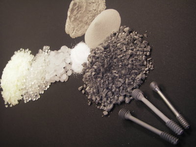 |
| Metal powder injection molding: Top right the metal powders and polymer components left, center: the mixed Granualt. Below: component precursors, and the final Mg-Ca-bone screw to the right. [Photo:HZG/M. Wolff] |
Is a paradigm shift imminent in the field of implant materials? Scientists at the Helmholtz Zentrum Geesthacht are engaged in research on biodegradable magnesium biomaterials which can be used as bone replacements in medical applications. They will present their research results from the 1st to 3rd November at the annual congress of the DGBM (German society for Biomaterials) in Hamburg.
When autumn arrives it brings wind and rain, leaves fall from the trees and settle on the ground. If someone slips on them, a bone can easily be broken. When a nail or a plate is required for the fixation of such a bone fracture, it is nowadays usually made of titanium, as this material is stable and well-tolerated by the human body. However, this foreign body must often be removed after the bone has healed, as there is otherwise a danger of inflammation or even bone loss.
According to Prof. Dr. Regine Willumeit, the head of the ‘Structural Research on Macromolecules’ department at the Helmholtz-Zentrum Geesthacht: “The aim of modern implant research is to develop a material which can be used in the body like a real replacement material. A biomaterial which at first supports the bone but then disappears of its own accord after the bone has recovered”.
Magnesium is excellently suited to this purpose. This element is naturally present in the human body and has the advantage that it can biodegrade in a pre-determined manner. It must, thereby, be both light and strong but also well-tolerated by the body. Research scientists at the Helmholtz-Zentrum in Geesthacht are therefore focussing their attention on this particular biomaterial.
The Helmholtz-Zentrum in Geesthacht has shown great expertise for many years in the research and production of prototypes for metallic biodegradable magnesium alloy implants. Material researchers are, for example, engaged in investigations into innovative magnesium-calcium alloys. These reveal material properties similar to those in bone; they are firm and at the same time elastic. Calcium appears to be well suited as an alloy as it would be able to degrade into non-toxic products in the body in the same way as magnesium. The degradation products would even be able to stimulate bone growth.
As Prof. Dr. Regine Willumeit explains: “ We are developing alloys in Geesthacht which have extremely promising properties for use in orthopaedic and traumatological applications. The colleagues at the Magnesium Innovations Center, MagIC, at the HZG, provide us with the starting material, we examine the factors which determine the degradation of the magnesium under physiological conditions”.
Scientists are not only engaged in research into the degradation process of the material itself. Tests are carried out in the Geesthacht laboratories in cell culture on the effects of the degradation on surrounding cells, for example. The scientists involved in this fundamental research into innovative implant materials have comprehensive analysis and test methods at their disposal.
As stable as bone, yet with good biodegradability
 |
| Would spare the second operation for removal of screws and plates: implant material of biodegradable magnesium [Photo: Istock 21545233] |
The development of production processes is still causing researchers headaches. However, they have also made great progress in this area. The scientist Martin Wolff, from the powder technology department, has, for the first time, succeeded in producing magnesium-calcium bone screws by means of the metal powder injection molding process (MIM).
As he explains: “The challenge in the case of magnesium lies in the high affinity of this material for oxygen. However, even small amounts of oxygen lead to dramatic changes in the mechanical properties of the component. Calcium, as an alloy partner, captures the oxygen in the production process during the so-called sintering procedure, and the material thus becomes firmer. This non-toxic alloying element has proved successful in achieving better results, at least in experiments. However, numerous further investigations now lie ahead, e.g. in cell culture and in the organism, before this material can be utilized as an implant material.
The Helmholtz researchers from Geesthacht will present their results at the Annual Congress of the Deutsche Gesellschaft für Biomaterialien, DGBM (German Society for Biomaterials), which is to be held at the Chamber of Commerce in Hamburg from 1st to 3rd of November 2012. The main focus this year will be on “Degradable Implants and Biomaterials”. The Congress will be led by Prof. Dr. Regine Willumeit.
Source: Helmholtz Zentrum Geesthacht
Additional Information:
Poster Rapid Fire Presentation
New format for the presentation of research results. The scientist’s
own research field and results must be clearly presented in only five
minutes.
Metal powder injection moulding MIM
MIM uses injection moulding technology for the shaping process, which
is also widely used in the field of plastics. The starting material is a
fine metal powder which is mixed with a so-called binder. This mixture
is fused at approx. 100 degrees centigrade. The binder is then
chemically removed from the injection moulded part so that only the
metal remains. The powder is compacted to the desired firm and dense
body by means of a sintering process.
Friday, 26 October 2012
Reclaiming rare earths: Laboratory improving process to recycle rare-earth materials
Engineerblogger
Oct 26, 2012
Recycling keeps paper, plastics, and even jeans out of landfills. Could recycling rare-earth magnets do the same? Perhaps, if the recycling process can be improved.
Scientists at the U.S. Department of Energy’s (DOE) Ames Laboratory are working to more effectively remove the neodymium, a rare earth element, from the mix of other materials in a magnet. Initial results show recycled materials maintain the properties that make rare-earth magnets useful.
The current rare earth recycling research builds on Ames Laboratory’s decades of rare-earth processing experience. In the 1990s, Ames Lab scientists developed a process that uses molten magnesium to remove rare earths from neodymium-iron-boron magnet scrap. Back then, the goal was to produce a mixture of magnesium and neodymium because the neodymium added important strength to the alloy, rather than separate out high-purity rare earths because, at the time, rare earth prices were low.
But rare earth prices increased ten-fold between 2009 and 2011 and supplies are in question. Therefore, the goal of today’s rare-earth recycling research takes the process one step farther.
“Now the goal is to make new magnet alloys from recycled rare earths. And we want those new alloys to be similar to alloys made from unprocessed rare-earth materials,” said Ryan Ott, the Ames Laboratory scientist leading the research. “It appears that the processing technique works well. It effectively removes rare earths from commercial magnets.”
Ott’s research team also includes Ames Laboratory scientist Larry Jones and is funded through a work for others agreement with the Korea Institute of Industrial Technology. The research group is developing and testing the technique in Ames Lab’s Materials Preparation Center, with a suite of materials science tools supported by the DOE Office of Science.
“We start with sintered, uncoated magnets that contain three rare earths: neodymium, praseodymium and dysprosium,” said Ott. “Then we break up the magnets in an automated mortar and pestle until the pieces are 2-4 millimeters long.
Next, the tiny magnet pieces go into a mesh screen box, which is placed in a stainless-steel crucible. Technicians then add chunks of solid magnesium.
A radio frequency furnace heats the material. The magnesium begins to melt, while the magnet chunks remain solid.
“What happens then is that all three rare earths leave the magnetic material by diffusion and enter the molten magnesium,” said Ott. “The iron and boron that made up the original magnet are left behind.”
The molten magnesium and rare-earth mixture is cast into an ingot and cooled. Then they boil off the magnesium, leaving just the rare earth materials behind.
“We’ve found that the properties of the recycled rare earths compare very favorably to ones from unprocessed materials,” said Ott. “We’re continuing to identify the ideal processing conditions.”
The next step is optimizing the extraction process. Then the team plans to demonstrate it on a larger scale.
“We want to help bridge the gap between the fundamental science and using this science in manufacturing,” said Ott. “And Ames Lab can process big enough amounts of material to show that our rare-earth recycling process works on a large scale.”
Source: Ames Laboratory
Oct 26, 2012
 |
| Rare-earth magnet scraps are melted in a furnace with magnesium. Scientists at the Ames Laboratory are improving the process to reclaim rare-earth materials. |
Recycling keeps paper, plastics, and even jeans out of landfills. Could recycling rare-earth magnets do the same? Perhaps, if the recycling process can be improved.
Scientists at the U.S. Department of Energy’s (DOE) Ames Laboratory are working to more effectively remove the neodymium, a rare earth element, from the mix of other materials in a magnet. Initial results show recycled materials maintain the properties that make rare-earth magnets useful.
The current rare earth recycling research builds on Ames Laboratory’s decades of rare-earth processing experience. In the 1990s, Ames Lab scientists developed a process that uses molten magnesium to remove rare earths from neodymium-iron-boron magnet scrap. Back then, the goal was to produce a mixture of magnesium and neodymium because the neodymium added important strength to the alloy, rather than separate out high-purity rare earths because, at the time, rare earth prices were low.
But rare earth prices increased ten-fold between 2009 and 2011 and supplies are in question. Therefore, the goal of today’s rare-earth recycling research takes the process one step farther.
“Now the goal is to make new magnet alloys from recycled rare earths. And we want those new alloys to be similar to alloys made from unprocessed rare-earth materials,” said Ryan Ott, the Ames Laboratory scientist leading the research. “It appears that the processing technique works well. It effectively removes rare earths from commercial magnets.”
Ott’s research team also includes Ames Laboratory scientist Larry Jones and is funded through a work for others agreement with the Korea Institute of Industrial Technology. The research group is developing and testing the technique in Ames Lab’s Materials Preparation Center, with a suite of materials science tools supported by the DOE Office of Science.
“We start with sintered, uncoated magnets that contain three rare earths: neodymium, praseodymium and dysprosium,” said Ott. “Then we break up the magnets in an automated mortar and pestle until the pieces are 2-4 millimeters long.
Next, the tiny magnet pieces go into a mesh screen box, which is placed in a stainless-steel crucible. Technicians then add chunks of solid magnesium.
A radio frequency furnace heats the material. The magnesium begins to melt, while the magnet chunks remain solid.
“What happens then is that all three rare earths leave the magnetic material by diffusion and enter the molten magnesium,” said Ott. “The iron and boron that made up the original magnet are left behind.”
The molten magnesium and rare-earth mixture is cast into an ingot and cooled. Then they boil off the magnesium, leaving just the rare earth materials behind.
“We’ve found that the properties of the recycled rare earths compare very favorably to ones from unprocessed materials,” said Ott. “We’re continuing to identify the ideal processing conditions.”
The next step is optimizing the extraction process. Then the team plans to demonstrate it on a larger scale.
“We want to help bridge the gap between the fundamental science and using this science in manufacturing,” said Ott. “And Ames Lab can process big enough amounts of material to show that our rare-earth recycling process works on a large scale.”
Source: Ames Laboratory
Electron 'sniper' targets graphene
Engineerblogger
Oct 26, 2012
Because of its intriguing properties graphene could be the ideal material for building new kinds of electronic devices such as sensors, screens, or even quantum computers.
One of the keys to exploiting graphene's potential is being able to create atomic-scale defects – where carbon atoms in its flat, honeycomb-like structure are rearranged or 'knocked out' – as these influence its electrical, chemical, magnetic, and mechanical properties.
A team led by Oxford University scientists report in Nature Communications a new approach to a new approach to engineering graphene's atomic structure with unprecedented precision.
'Current approaches for producing defects in graphene are either like a 'shotgun' where the entire sample is sprayed with high energy ions or electrons to cause widespread defects, or a chemistry approach where many regions of the graphene are chemically reacted,' said Jamie Warner from Oxford University's Department of Materials, a member of the team.
'Both methods lack any form of control in terms of spatial precision and also the defect type, but to date are the only reported methods known for defect creation.'
The new method replaces the 'shotgun' with something more like a sniper rifle: a minutely-controlled beam of electrons fired from an electron microscope.
'The shotgun approach is restricted to micron scale precision, which is roughly an area of 10,000,000 square nanometres, we demonstrated a precision to within 100 square nanometres, which is about four orders of magnitude better,' explains Alex Robertson of Oxford University's Department of Materials, another member of the team.
Yet it isn’t just about the accuracy of a single 'shot'; the researchers also show that by controlling the length of time graphene is exposed to their focused beam of electrons they can control the size and type of defect created.
'Our study reveals for the first time that only a few types of defects are actually stable in graphene, with several defects being quenched by surface atoms or relaxing back to pristine by bond rotations,' Jamie tells me.
The ability to create just the right kind of stable defects in graphene's crystal structure is going to be vital if its properties are to be harnessed for applications such as mobile phones and flexible displays.
'Defect sites in graphene are much more chemically reactive, so we can use defects as a site for chemical functionalisation of the graphene. So we can attach certain molecules, such as biomolecules, to the graphene to act as a sensor,' Alex tells me.
'Defects in graphene can also give rise to localized electron spin, an attribute that has important future use in quantum nanotechnology and quantum computers.'
At the moment scaling up the team's technique into a manufacturing process to create graphene-based technologies is still a way off. Currently electron microscopes are the only systems that can achieve the necessary exquisite control of an electron beam.
But, Alex says, it is always possible that a scalable electron beam lithography type technique may be developed in the future that could allow for defect patterning in graphene.And it's worth remembering that it wasn't so long ago that the technology needed to etch millions of transistors onto a tiny slice of silicon seemed like an impossible dream.
Source: Oxford University
Additional Information:
Oct 26, 2012
 |
| Credit: Oxford University |
Because of its intriguing properties graphene could be the ideal material for building new kinds of electronic devices such as sensors, screens, or even quantum computers.
One of the keys to exploiting graphene's potential is being able to create atomic-scale defects – where carbon atoms in its flat, honeycomb-like structure are rearranged or 'knocked out' – as these influence its electrical, chemical, magnetic, and mechanical properties.
A team led by Oxford University scientists report in Nature Communications a new approach to a new approach to engineering graphene's atomic structure with unprecedented precision.
'Current approaches for producing defects in graphene are either like a 'shotgun' where the entire sample is sprayed with high energy ions or electrons to cause widespread defects, or a chemistry approach where many regions of the graphene are chemically reacted,' said Jamie Warner from Oxford University's Department of Materials, a member of the team.
'Both methods lack any form of control in terms of spatial precision and also the defect type, but to date are the only reported methods known for defect creation.'
The new method replaces the 'shotgun' with something more like a sniper rifle: a minutely-controlled beam of electrons fired from an electron microscope.
'The shotgun approach is restricted to micron scale precision, which is roughly an area of 10,000,000 square nanometres, we demonstrated a precision to within 100 square nanometres, which is about four orders of magnitude better,' explains Alex Robertson of Oxford University's Department of Materials, another member of the team.
Yet it isn’t just about the accuracy of a single 'shot'; the researchers also show that by controlling the length of time graphene is exposed to their focused beam of electrons they can control the size and type of defect created.
'Our study reveals for the first time that only a few types of defects are actually stable in graphene, with several defects being quenched by surface atoms or relaxing back to pristine by bond rotations,' Jamie tells me.
The ability to create just the right kind of stable defects in graphene's crystal structure is going to be vital if its properties are to be harnessed for applications such as mobile phones and flexible displays.
'Defect sites in graphene are much more chemically reactive, so we can use defects as a site for chemical functionalisation of the graphene. So we can attach certain molecules, such as biomolecules, to the graphene to act as a sensor,' Alex tells me.
'Defects in graphene can also give rise to localized electron spin, an attribute that has important future use in quantum nanotechnology and quantum computers.'
At the moment scaling up the team's technique into a manufacturing process to create graphene-based technologies is still a way off. Currently electron microscopes are the only systems that can achieve the necessary exquisite control of an electron beam.
But, Alex says, it is always possible that a scalable electron beam lithography type technique may be developed in the future that could allow for defect patterning in graphene.And it's worth remembering that it wasn't so long ago that the technology needed to etch millions of transistors onto a tiny slice of silicon seemed like an impossible dream.
Source: Oxford University
Additional Information:
Sunday, 9 September 2012
Honda Develops New Technology to Weld Together Steel and Aluminum and Achieves World's First Application to the Frame of a Mass-production Vehicle
Engineerblogger
Sept. 9, 2012
Honda Motor Company announced that it has newly developed a technology for the continuous welding of the dissimilar metals of steel and aluminum and applied it for the first time in the world to the subframe of a mass-production vehicle, a key component of a vehicle body frame. Honda will adopt this technology first to the North American version of the all-new 2013 Accord, which will go on sale in the United States on September 19, 2012, and will expand application sequentially to other models.
Striving to reduce vehicle weight in order to increase fuel economy, Honda focused on Friction Stir Welding (FSW) and developed a new technology for the continuous welding of steel and aluminum. This technology generates a new and stable metallic bonding between steel and aluminum by moving a rotating tool on the top of the aluminum which is lapped over the steel with high pressure. As a result, the welding strength becomes equal to or beyond conventional Metal Inert Gas (MIG) welding*1.
This new technology contributes to an improvement in fuel economy by reducing body weight by 25% compared to a conventional steel subframe. In addition, electricity consumption during the welding process is reduced by approximately 50%. It also enabled a change in the structure of the subframe and the mounting point of suspension, which increased the rigidity of the mounting point by 20% and also contributed to the vehicle’s dynamic performance.
Furthermore, Honda established a new method to apply this technology to mass-production vehicles. Conventionally, FSW required use of large equipment, but Honda developed a FSW continuous welding system applied to a highly versatile industrial robot. This system also can be used for aluminum-to-aluminum welding and thus, the welding system with the same specifications can be used for production of a full-aluminum subframe.
Honda also developed a non-destructive inspection system*2 using a highly-sensitive infrared camera and laser beam, which enables an in-line inspection of the bonding location for every unit.
*1 A welding technique most commonly used for welding of identical materials such as steel-to-steel or aluminum-to-aluminum
*2A system that evaluates quality without actually destructing the parts
Source: Honda
Sept. 9, 2012
 |
| Front Subframe |
Honda Motor Company announced that it has newly developed a technology for the continuous welding of the dissimilar metals of steel and aluminum and applied it for the first time in the world to the subframe of a mass-production vehicle, a key component of a vehicle body frame. Honda will adopt this technology first to the North American version of the all-new 2013 Accord, which will go on sale in the United States on September 19, 2012, and will expand application sequentially to other models.
 |
| Conceptual diagram of FSW of dissimilar metals |
Striving to reduce vehicle weight in order to increase fuel economy, Honda focused on Friction Stir Welding (FSW) and developed a new technology for the continuous welding of steel and aluminum. This technology generates a new and stable metallic bonding between steel and aluminum by moving a rotating tool on the top of the aluminum which is lapped over the steel with high pressure. As a result, the welding strength becomes equal to or beyond conventional Metal Inert Gas (MIG) welding*1.
This new technology contributes to an improvement in fuel economy by reducing body weight by 25% compared to a conventional steel subframe. In addition, electricity consumption during the welding process is reduced by approximately 50%. It also enabled a change in the structure of the subframe and the mounting point of suspension, which increased the rigidity of the mounting point by 20% and also contributed to the vehicle’s dynamic performance.
Furthermore, Honda established a new method to apply this technology to mass-production vehicles. Conventionally, FSW required use of large equipment, but Honda developed a FSW continuous welding system applied to a highly versatile industrial robot. This system also can be used for aluminum-to-aluminum welding and thus, the welding system with the same specifications can be used for production of a full-aluminum subframe.
Honda also developed a non-destructive inspection system*2 using a highly-sensitive infrared camera and laser beam, which enables an in-line inspection of the bonding location for every unit.
*1 A welding technique most commonly used for welding of identical materials such as steel-to-steel or aluminum-to-aluminum
*2A system that evaluates quality without actually destructing the parts
Source: Honda
Could ancient Egyptians hold the key to 3D printed ceramics?
Engineerblogger
Sept 3, 2012
Video: Professor Stephen Hoskins shares more about the latest 3D printing methods in ceramics in this insightful interview.
A 7,000 year old technique, known as Egyptian Paste (also known as Faience), could offer a potential process and material for use in the latest 3D printing techniques of ceramics, according to researchers at UWE Bristol.
Professor Stephen Hoskins, Director of UWE's Centre for Fine Print Research and David Huson, Research Fellow, have received funding from the Arts and Humanities Research Council (AHRC to undertake a major investigation into a self-glazing 3D printed ceramic, inspired by ancient Egyptian Faience ceramic techniques. The process they aim to develop would enable ceramic artists, designers and craftspeople to print 3D objects in a ceramic material which can be glazed and vitrified in one firing.
The researchers believe that it possible to create a contemporary 3D printable, once-fired, self-glazing, non-plastic ceramic material that exhibits the characteristics and quality of Egyptian Faience.
Faience was first used in the 5th Millennium BC and was the first glazed ceramic material invented by man. Faience was not made from clay (but instead composed of quartz and alkali fluxes) and is distinct from Italian Faience or Majolica, which is a tin, glazed earthenware. (The earliest Faience is invariably blue or green, exhibiting the full range of shades between them, and the colouring material was usually copper). It is the self-glazing properties of Faience that are of interest for this research project.
Current research in the field of 3D printing concentrates on creating functional materials to form physical models. The materials currently used in the 3D printing process, in which layers are added to build up a 3D form, are commonly: UV polymer resins, hot melted 'abs' plastic and inkjet binder or laser sintered, powder materials. These techniques have previously been known as rapid prototyping (RP). With the advent of better materials and equipment some RP of real materials is now possible. These processes are increasingly being referred to as solid 'free-form fabrication' (SFF) or additive layer manufacture. The UWE research team have focused previously on producing a functional, printable clay body.
This three-year research project will investigate three methods of glazing used by the ancient Egyptians: 'application glazing', similar to modern glazing methods; 'efflorescent glazing' which uses water-soluble salts; and 'cementation glazing', a technique where the object is buried in a glazing powder in a protective casing, then fired.These techniques will be used as a basis for developing contemporary printable alternatives
Professor Hoskins explains, “It is fascinating to think that some of these ancient processes, in fact the very first glazed ceramics every created by humans, could have relevance to the advanced printing technology of today. We hope to create a self-glazing 3D printed ceramic which only requires one firing from conception to completion rather than the usual two. This would be a radical step-forward in the development of 3D printing technologies. As part of the project we will undertake case studies of craft, design and fine art practitioners to contribute to the project, so that our work reflects the knowledge and understanding of artists and reflects the way in which artists work.”
The project includes funding for a three-year full-time PhD bursary to research a further method used by the Egyptians, investigating coloured 'frit', a substance used in glazing and enamels. This student will research this method, investigating the use of coloured frits and oxides to try and create as full a colour range as possible. Once developed, this body will be used to create a ceramic extrusion paste that can be printed with a low-cost 3D printer. A programme of work will be undertaken to determine the best rates of deposition, the inclusion of flocculants and methods of drying through heat whilst printing.
This project offers the theoretical possibility of a printed, single fired, glazed ceramic object - something that is impossible with current technology.
Source: University of the West of England
Sept 3, 2012
Video: Professor Stephen Hoskins shares more about the latest 3D printing methods in ceramics in this insightful interview.
A 7,000 year old technique, known as Egyptian Paste (also known as Faience), could offer a potential process and material for use in the latest 3D printing techniques of ceramics, according to researchers at UWE Bristol.
Professor Stephen Hoskins, Director of UWE's Centre for Fine Print Research and David Huson, Research Fellow, have received funding from the Arts and Humanities Research Council (AHRC to undertake a major investigation into a self-glazing 3D printed ceramic, inspired by ancient Egyptian Faience ceramic techniques. The process they aim to develop would enable ceramic artists, designers and craftspeople to print 3D objects in a ceramic material which can be glazed and vitrified in one firing.
The researchers believe that it possible to create a contemporary 3D printable, once-fired, self-glazing, non-plastic ceramic material that exhibits the characteristics and quality of Egyptian Faience.
Faience was first used in the 5th Millennium BC and was the first glazed ceramic material invented by man. Faience was not made from clay (but instead composed of quartz and alkali fluxes) and is distinct from Italian Faience or Majolica, which is a tin, glazed earthenware. (The earliest Faience is invariably blue or green, exhibiting the full range of shades between them, and the colouring material was usually copper). It is the self-glazing properties of Faience that are of interest for this research project.
Current research in the field of 3D printing concentrates on creating functional materials to form physical models. The materials currently used in the 3D printing process, in which layers are added to build up a 3D form, are commonly: UV polymer resins, hot melted 'abs' plastic and inkjet binder or laser sintered, powder materials. These techniques have previously been known as rapid prototyping (RP). With the advent of better materials and equipment some RP of real materials is now possible. These processes are increasingly being referred to as solid 'free-form fabrication' (SFF) or additive layer manufacture. The UWE research team have focused previously on producing a functional, printable clay body.
This three-year research project will investigate three methods of glazing used by the ancient Egyptians: 'application glazing', similar to modern glazing methods; 'efflorescent glazing' which uses water-soluble salts; and 'cementation glazing', a technique where the object is buried in a glazing powder in a protective casing, then fired.These techniques will be used as a basis for developing contemporary printable alternatives
Professor Hoskins explains, “It is fascinating to think that some of these ancient processes, in fact the very first glazed ceramics every created by humans, could have relevance to the advanced printing technology of today. We hope to create a self-glazing 3D printed ceramic which only requires one firing from conception to completion rather than the usual two. This would be a radical step-forward in the development of 3D printing technologies. As part of the project we will undertake case studies of craft, design and fine art practitioners to contribute to the project, so that our work reflects the knowledge and understanding of artists and reflects the way in which artists work.”
The project includes funding for a three-year full-time PhD bursary to research a further method used by the Egyptians, investigating coloured 'frit', a substance used in glazing and enamels. This student will research this method, investigating the use of coloured frits and oxides to try and create as full a colour range as possible. Once developed, this body will be used to create a ceramic extrusion paste that can be printed with a low-cost 3D printer. A programme of work will be undertaken to determine the best rates of deposition, the inclusion of flocculants and methods of drying through heat whilst printing.
This project offers the theoretical possibility of a printed, single fired, glazed ceramic object - something that is impossible with current technology.
Source: University of the West of England
Boaz Almog “levitates” a superconductor
Engineerblogger
Sept 9, 2012
How can a super-thin 3-inch disk levitate something 70,000 times its own weight? In a riveting demonstration, Boaz Almog shows how a phenomenon known as quantum locking allows a superconductor disk to float over a magnetic rail -- completely frictionlessly and with zero energy loss.
Experiment: Prof. Guy Deutscher, Mishael Azoulay, Boaz Almog, of the High Tc Superconductivity Group, School of Physics and Astronomy, Tel Aviv University.
Source: TED
Sept 9, 2012
How can a super-thin 3-inch disk levitate something 70,000 times its own weight? In a riveting demonstration, Boaz Almog shows how a phenomenon known as quantum locking allows a superconductor disk to float over a magnetic rail -- completely frictionlessly and with zero energy loss.
Experiment: Prof. Guy Deutscher, Mishael Azoulay, Boaz Almog, of the High Tc Superconductivity Group, School of Physics and Astronomy, Tel Aviv University.
Source: TED
Saturday, 8 September 2012
Reference Material Could Aid Nanomaterial Toxicity Research
Engineerblogger
Sept 9, 2012
The National Institute of Standards and Technology (NIST) has issued a new nanoscale reference material for use in a wide range of environmental, health and safety studies of industrial nanomaterials. The new NIST reference material is a sample of commercial titanium dioxide powder commonly known as “P25.”
NIST Standard Reference Materials® (SRMs) are typically samples of industrially or clinically important materials that have been carefully analyzed by NIST. They are provided with certified values for certain key properties so that they can be used in experiments as a known reference point.
Nanoscale titanium-dioxide powder may well be the most widely manufactured and used nanomaterial in the world, and not coincidentally, it is also one of the most widely studied. In the form of larger particles, titanium dioxide is a common white pigment. As nanoscale particles, the material is widely used as a photocatalyst, a sterilizing agent and an ultraviolet blocker (in sunscreen lotions, for example).
“Titanium dioxide is not considered highly toxic and, in fact, we don’t certify its toxicity,” observes NIST chemist Vincent Hackley. “But it’s a representative industrial nanopowder that you could include in an environmental or toxicity study. It’s important in such research to include measurements that characterize the nanomaterial you’re studying—properties like morphology, surface area and elemental composition. We’re providing a known benchmark.”
The new titanium-dioxide reference material is a mixed phase, nanocrystalline form of the chemical in a dry powder. To assist in its proper use, NIST also has developed protocols* for properly preparing samples for environmental or toxicological studies.
The new SRM also is particularly well suited for use in calibrating and testing analytical instruments that measure specific surface area of nanomaterials by the widely used Brunauer-Emmet-Teller (BET) gas sorption method.
Additional details and purchasing information on NIST Standard Reference Material 1898, “Titanium Dioxide Nanomaterial” are available at www.nist.gov/srm/index.cfm.
SRMs are among the most widely distributed and used products from NIST. The agency prepares, analyzes and distributes nearly 1,300 different materials that are used throughout the world to check the accuracy of instruments and test procedures used in manufacturing, clinical chemistry, environmental monitoring, electronics, criminal forensics and dozens of other fields.
Source: The National Institute of Standards and Technology (NIST)
Additional Information:
Sept 9, 2012
 |
TEM image shows the nanoscale crystalline structure of titanium dioxide in NIST SRM 1898 (color added for clarity.) Credit: Impellitteri/EPA |
NIST Standard Reference Materials® (SRMs) are typically samples of industrially or clinically important materials that have been carefully analyzed by NIST. They are provided with certified values for certain key properties so that they can be used in experiments as a known reference point.
Nanoscale titanium-dioxide powder may well be the most widely manufactured and used nanomaterial in the world, and not coincidentally, it is also one of the most widely studied. In the form of larger particles, titanium dioxide is a common white pigment. As nanoscale particles, the material is widely used as a photocatalyst, a sterilizing agent and an ultraviolet blocker (in sunscreen lotions, for example).
“Titanium dioxide is not considered highly toxic and, in fact, we don’t certify its toxicity,” observes NIST chemist Vincent Hackley. “But it’s a representative industrial nanopowder that you could include in an environmental or toxicity study. It’s important in such research to include measurements that characterize the nanomaterial you’re studying—properties like morphology, surface area and elemental composition. We’re providing a known benchmark.”
The new titanium-dioxide reference material is a mixed phase, nanocrystalline form of the chemical in a dry powder. To assist in its proper use, NIST also has developed protocols* for properly preparing samples for environmental or toxicological studies.
The new SRM also is particularly well suited for use in calibrating and testing analytical instruments that measure specific surface area of nanomaterials by the widely used Brunauer-Emmet-Teller (BET) gas sorption method.
Additional details and purchasing information on NIST Standard Reference Material 1898, “Titanium Dioxide Nanomaterial” are available at www.nist.gov/srm/index.cfm.
SRMs are among the most widely distributed and used products from NIST. The agency prepares, analyzes and distributes nearly 1,300 different materials that are used throughout the world to check the accuracy of instruments and test procedures used in manufacturing, clinical chemistry, environmental monitoring, electronics, criminal forensics and dozens of other fields.
Source: The National Institute of Standards and Technology (NIST)
Additional Information:
- See “Protocols for Measurement and Dispersion of Nanoparticles” at www.nist.gov/mml/np-measurement-protocols.cfm.
Researchers Set World Record for Highest Surface Area Material
Engineerblogger
Sept 9, 2012
Northwestern University researchers have broken a world record by creating two new synthetic materials with the greatest amount of surface areas reported to date.
Named NU-109 and NU-110, the materials belong to a class of crystalline nanostructure known as metal-organic frameworks (MOFs) that are promising vessels for natural gas storage for vehicles, catalysts, and other sustainable materials chemistry.
The materials’ promise lies in their vast internal surface area. If the internal surface area of one NU-110 crystal the size of a grain of salt could be unfolded, the surface area would cover a desktop. Put another way, the internal surface area of one gram of NU-110 would cover one-and-a-half football fields.
A paper describing the findings, “Metal-organic Framework Materials with Ultrahigh Surface Areas: Is the Sky the Limit?” was published August 20 in the Journal of the American Chemical Society.
The research team, led by Omar Farha, research associate professor of chemistry in the Weinberg College of Arts and Sciences, has synthesized, characterized, and computationally simulated the behavior of the two MOFs that display the highest experimental Brunauer-Emmett-Teller surface areas of any porous material on record, 7,000 m2/g; that is, one kilogram of the material contains an internal surface area that could cover seven square kilometers. (Brunauer-Emmett-Teller, or BET, is an analysis technique for measuring the surface area of a material.)
The extremely high surface area, which is normally not accessible due to solvent molecules that stay trapped within the pores, was achieved using a carbon dioxide activation technique. As opposed to heating, which can remove the solvent but also damage the MOF material, the carbon dioxide-based technique removes the solvent gently and leaves the pores completely intact.
The development could rapidly lead to further advances. MOFs are composed of organic linkers held together by metal atoms, resulting in a molecular cage-like structure. The researchers believe they may be able to more than double the surface area of the materials by using less bulky linker units in the materials’ design.
The research comes from the labs of Joseph T. Hupp, professor of chemistry in Weinberg, and Randall Q. Snurr, professor of chemical and biological engineering at the McCormick School of Engineering.
Other authors include SonBinh Nguyen, professor of chemistry in Weinberg; Ibrahim Eryazici, Nak Cheon Jeong, Brad G. Hauser, Amy A. Sarjeant, and Christopher E. Wilmer, all of Northwestern; and A. Özgür Yazaydın of the University of Surrey in the United Kingdom.
The MOF-designing and -synthesizing technology is being commercialized by NuMat Technologies, a Northwestern startup that has won more than $1 million in business plan competitions since incorporating in February.
Source: Northwestern University
Sept 9, 2012
Northwestern University researchers have broken a world record by creating two new synthetic materials with the greatest amount of surface areas reported to date.
Named NU-109 and NU-110, the materials belong to a class of crystalline nanostructure known as metal-organic frameworks (MOFs) that are promising vessels for natural gas storage for vehicles, catalysts, and other sustainable materials chemistry.
The materials’ promise lies in their vast internal surface area. If the internal surface area of one NU-110 crystal the size of a grain of salt could be unfolded, the surface area would cover a desktop. Put another way, the internal surface area of one gram of NU-110 would cover one-and-a-half football fields.
A paper describing the findings, “Metal-organic Framework Materials with Ultrahigh Surface Areas: Is the Sky the Limit?” was published August 20 in the Journal of the American Chemical Society.
The research team, led by Omar Farha, research associate professor of chemistry in the Weinberg College of Arts and Sciences, has synthesized, characterized, and computationally simulated the behavior of the two MOFs that display the highest experimental Brunauer-Emmett-Teller surface areas of any porous material on record, 7,000 m2/g; that is, one kilogram of the material contains an internal surface area that could cover seven square kilometers. (Brunauer-Emmett-Teller, or BET, is an analysis technique for measuring the surface area of a material.)
The extremely high surface area, which is normally not accessible due to solvent molecules that stay trapped within the pores, was achieved using a carbon dioxide activation technique. As opposed to heating, which can remove the solvent but also damage the MOF material, the carbon dioxide-based technique removes the solvent gently and leaves the pores completely intact.
The development could rapidly lead to further advances. MOFs are composed of organic linkers held together by metal atoms, resulting in a molecular cage-like structure. The researchers believe they may be able to more than double the surface area of the materials by using less bulky linker units in the materials’ design.
The research comes from the labs of Joseph T. Hupp, professor of chemistry in Weinberg, and Randall Q. Snurr, professor of chemical and biological engineering at the McCormick School of Engineering.
Other authors include SonBinh Nguyen, professor of chemistry in Weinberg; Ibrahim Eryazici, Nak Cheon Jeong, Brad G. Hauser, Amy A. Sarjeant, and Christopher E. Wilmer, all of Northwestern; and A. Özgür Yazaydın of the University of Surrey in the United Kingdom.
The MOF-designing and -synthesizing technology is being commercialized by NuMat Technologies, a Northwestern startup that has won more than $1 million in business plan competitions since incorporating in February.
Source: Northwestern University
Friday, 3 August 2012
Transparent solar cells for windows that generate electricity
Engineerblogger
Aug 3, 2012
Scientists are reporting development of a new transparent solar cell, an advance toward giving windows in homes and other buildings the ability to generate electricity while still allowing people to see outside. Their report appears in the journal ACS Nano.
Yang Yang, Rui Zhu, Paul S. Weiss and colleagues explain that there has been intense world-wide interest in so-called polymer solar cells (PSCs), which are made from plastic-like materials. PSCs are lightweight and flexible and can be produced in high volume at low cost. That interest extends to producing transparent PSCs. However, previous versions of transparent PSCs have had many disadvantages, which the team set out to correct.
They describe a new kind of PSC that produces energy by absorbing mainly infrared light, not visible light, making the cells 66 percent transparent to the human eye. They made the device from a photoactive plastic that converts infrared light into an electrical current. Another breakthrough is the transparent conductor made of a mixture of silver nanowire and titanium dioxide nanoparticles, which was able to replace the opaque metal electrode used in the past. This composite electrode also allowed the solar cell to be fabricated economically by solution processing. The authors suggest the panels could be used in smart windows or portable electronics.
The authors acknowledge funding from the Engineering School of UCLA, the Office of Naval Research and the Kavli Foundation.
Aug 3, 2012
 |
Visibly transparent photovoltaic devices can open photovoltaic applications in many areas, such as building-integrated photovoltaics or integrated photovoltaic chargers for portable electronics. We demonstrate high-performance, visibly transparent polymer solar cells fabricated via solution processing. The photoactive layer of these visibly transparent polymer solar cells harvests solar energy from the near-infrared region while being less sensitive to visible photons. The top transparent electrode employs a highly transparent silver nanowire–metal oxide composite conducting film, which is coated through mild solution processes. With this combination, we have achieved 4% power-conversion efficiency for solution-processed and visibly transparent polymer solar cells. The optimized devices have a maximum transparency of 66% at 550 nm. |
Scientists are reporting development of a new transparent solar cell, an advance toward giving windows in homes and other buildings the ability to generate electricity while still allowing people to see outside. Their report appears in the journal ACS Nano.
Yang Yang, Rui Zhu, Paul S. Weiss and colleagues explain that there has been intense world-wide interest in so-called polymer solar cells (PSCs), which are made from plastic-like materials. PSCs are lightweight and flexible and can be produced in high volume at low cost. That interest extends to producing transparent PSCs. However, previous versions of transparent PSCs have had many disadvantages, which the team set out to correct.
They describe a new kind of PSC that produces energy by absorbing mainly infrared light, not visible light, making the cells 66 percent transparent to the human eye. They made the device from a photoactive plastic that converts infrared light into an electrical current. Another breakthrough is the transparent conductor made of a mixture of silver nanowire and titanium dioxide nanoparticles, which was able to replace the opaque metal electrode used in the past. This composite electrode also allowed the solar cell to be fabricated economically by solution processing. The authors suggest the panels could be used in smart windows or portable electronics.
The authors acknowledge funding from the Engineering School of UCLA, the Office of Naval Research and the Kavli Foundation.
Source: American Chemical Society
Additional Information:
Thursday, 19 July 2012
Why platinum is the wrong material for fuel cell?
Engineerblogger
July 19, 2012
July 19, 2012
 |
| Professor Alfred Anderson |
Fuel cells are inefficient because the catalyst most commonly used to convert chemical energy to electricity is made of the wrong material, a researcher at Case Western Reserve University argues. Rather than continue the futile effort to tweak that material—platinum—to make it work better, Chemistry Professor Alfred Anderson urges his colleagues to start anew.
“Using platinum is like putting a resistor in the system,” he said. Anderson freely acknowledges he doesn’t know what the right material is, but he’s confident researchers’ energy would be better spent seeking it out than persisting with platinum.
“If we can find a catalyst that will do this [more efficiently],” he said, “it would reach closer to the limiting potential and get more energy out of the fuel cell.”
Anderson’s analysis and a guide for a better catalyst have been published in a recent issue of Physical Chemistry Chemical Physics and in Electrocatalysis online.
Even in the best of circumstances, Anderson explained, the chemical reaction that produces energy in a fuel cell—like those being tested by some car companies—ends up wasting a quarter of the energy that could be transformed into electricity. This point is well recognized in the scientific community, but, to date, efforts to address the problem have proved fruitless.
Anderson blames the failure on a fundamental misconception as to the reason for the energy waste. The most widely accepted theory says impurities are binding to the platinum surface of the cathode and blocking the desired reaction.
“The decades-old surface-poisoning explanation is lame because there is more to the story,” Anderson said.
To understand the loss of energy, Anderson used data derived from oxygen-reduction experiments to calculate the optimal bonding strengths between platinum and intermediate molecules formed during the oxygen-reduction reaction. The reaction takes place at the platinum-coated cathode.
He found the intermediate molecules bond too tightly or too loosely to the cathode surface, slowing the reaction and causing a drop in voltage. The result is the fuel cell produces about .93 volts instead of the potential maximum of 1.23 volts.
To eliminate the loss, calculations show, the catalyst should have bonding strengths tailored so that all reactions taking place during oxygen reduction occur at or as near to 1.23 volts as possible.
Anderson said the use of volcano plots, which are a statistical tool for comparing catalysts, has actually misguided the search for the best one. “They allow you to grade a series of similar catalysts, but they don’t point to better catalysts.”
He said a catalyst made of copper laccase, a material found in trees and fungi, has the desired bonding strength but lacks stability. Finding a catalyst that has both is the challenge.
Anderson is working with other researchers exploring alternative catalysts as well as an alternative reaction pathway in an effort to increase efficiency.
“Using platinum is like putting a resistor in the system,” he said. Anderson freely acknowledges he doesn’t know what the right material is, but he’s confident researchers’ energy would be better spent seeking it out than persisting with platinum.
“If we can find a catalyst that will do this [more efficiently],” he said, “it would reach closer to the limiting potential and get more energy out of the fuel cell.”
Anderson’s analysis and a guide for a better catalyst have been published in a recent issue of Physical Chemistry Chemical Physics and in Electrocatalysis online.
Even in the best of circumstances, Anderson explained, the chemical reaction that produces energy in a fuel cell—like those being tested by some car companies—ends up wasting a quarter of the energy that could be transformed into electricity. This point is well recognized in the scientific community, but, to date, efforts to address the problem have proved fruitless.
Anderson blames the failure on a fundamental misconception as to the reason for the energy waste. The most widely accepted theory says impurities are binding to the platinum surface of the cathode and blocking the desired reaction.
“The decades-old surface-poisoning explanation is lame because there is more to the story,” Anderson said.
To understand the loss of energy, Anderson used data derived from oxygen-reduction experiments to calculate the optimal bonding strengths between platinum and intermediate molecules formed during the oxygen-reduction reaction. The reaction takes place at the platinum-coated cathode.
He found the intermediate molecules bond too tightly or too loosely to the cathode surface, slowing the reaction and causing a drop in voltage. The result is the fuel cell produces about .93 volts instead of the potential maximum of 1.23 volts.
To eliminate the loss, calculations show, the catalyst should have bonding strengths tailored so that all reactions taking place during oxygen reduction occur at or as near to 1.23 volts as possible.
Anderson said the use of volcano plots, which are a statistical tool for comparing catalysts, has actually misguided the search for the best one. “They allow you to grade a series of similar catalysts, but they don’t point to better catalysts.”
He said a catalyst made of copper laccase, a material found in trees and fungi, has the desired bonding strength but lacks stability. Finding a catalyst that has both is the challenge.
Anderson is working with other researchers exploring alternative catalysts as well as an alternative reaction pathway in an effort to increase efficiency.
Source: Case Western Reserve University
Researchers Create Highly Conductive and Elastic Conductors Using Silver Nanowires
Engineerblogger
July 19, 2012
Researchers from North Carolina State University have developed highly conductive and elastic conductors made from silver nanoscale wires (nanowires). These elastic conductors can be used to develop stretchable electronic devices.
Stretchable circuitry would be able to do many things that its rigid counterpart cannot. For example, an electronic “skin” could help robots pick up delicate objects without breaking them, and stretchable displays and antennas could make cell phones and other electronic devices stretch and compress without affecting their performance. However, the first step toward making such applications possible is to produce conductors that are elastic and able to effectively and reliably transmit electric signals regardless of whether they are deformed.
Dr. Yong Zhu, an assistant professor of mechanical and aerospace engineering at NC State, and Feng Xu, a Ph.D. student in Zhu’s lab have developed such elastic conductors using silver nanowires.
Silver has very high electric conductivity, meaning that it can transfer electricity efficiently. And the new technique developed at NC State embeds highly conductive silver nanowires in a polymer that can withstand significant stretching without adversely affecting the material’s conductivity. This makes it attractive as a component for use in stretchable electronic devices.
“This development is very exciting because it could be immediately applied to a broad range of applications,” Zhu said. “In addition, our work focuses on high and stable conductivity under a large degree of deformation, complementary to most other work using silver nanowires that are more concerned with flexibility and transparency.”
“The fabrication approach is very simple,” says Xu. Silver nanowires are placed on a silicon plate. A liquid polymer is poured over the silicon substrate. The polymer is then exposed to high heat, which turns the polymer from a liquid into an elastic solid. Because the polymer flows around the silver nanowires when it is in liquid form, the nanowires are trapped in the polymer when it becomes solid. The polymer can then be peeled off the silicon plate.
“Also silver nanowires can be printed to fabricate patterned stretchable conductors,” Xu says. The fact that it is easy to make patterns using the silver nanowire conductors should facilitate the technique’s use in electronics manufacturing.
When the nanowire-embedded polymer is stretched and relaxed, the surface of the polymer containing nanowires buckles. The end result is that the composite is flat on the side that contains no nanowires, but wavy on the side that contains silver nanowires.
After the nanowire-embedded surface has buckled, the material can be stretched up to 50 percent of its elongation, or tensile strain, without affecting the conductivity of the silver nanowires. This is because the buckled shape of the material allows the nanowires to stay in a fixed position relative to each other, even as the polymer is being stretched.
“In addition to having high conductivity and a large stable strain range, the new stretchable conductors show excellent robustness under repeated mechanical loading,” Zhu says. Other reported stretchable conductive materials are typically deposited on top of substrates and could delaminate under repeated mechanical stretching or surface rubbing.
The paper, “Highly Conductive and Stretchable Silver Nanowire Conductors,” was published in Advanced Materials. The research was supported by the National Science Foundation.
Source: North Carolina State University
July 19, 2012
 |
The silver nanowires can be printed to fabricate patterned stretchable conductors.
|
Stretchable circuitry would be able to do many things that its rigid counterpart cannot. For example, an electronic “skin” could help robots pick up delicate objects without breaking them, and stretchable displays and antennas could make cell phones and other electronic devices stretch and compress without affecting their performance. However, the first step toward making such applications possible is to produce conductors that are elastic and able to effectively and reliably transmit electric signals regardless of whether they are deformed.
Dr. Yong Zhu, an assistant professor of mechanical and aerospace engineering at NC State, and Feng Xu, a Ph.D. student in Zhu’s lab have developed such elastic conductors using silver nanowires.
Silver has very high electric conductivity, meaning that it can transfer electricity efficiently. And the new technique developed at NC State embeds highly conductive silver nanowires in a polymer that can withstand significant stretching without adversely affecting the material’s conductivity. This makes it attractive as a component for use in stretchable electronic devices.
“This development is very exciting because it could be immediately applied to a broad range of applications,” Zhu said. “In addition, our work focuses on high and stable conductivity under a large degree of deformation, complementary to most other work using silver nanowires that are more concerned with flexibility and transparency.”
“The fabrication approach is very simple,” says Xu. Silver nanowires are placed on a silicon plate. A liquid polymer is poured over the silicon substrate. The polymer is then exposed to high heat, which turns the polymer from a liquid into an elastic solid. Because the polymer flows around the silver nanowires when it is in liquid form, the nanowires are trapped in the polymer when it becomes solid. The polymer can then be peeled off the silicon plate.
“Also silver nanowires can be printed to fabricate patterned stretchable conductors,” Xu says. The fact that it is easy to make patterns using the silver nanowire conductors should facilitate the technique’s use in electronics manufacturing.
When the nanowire-embedded polymer is stretched and relaxed, the surface of the polymer containing nanowires buckles. The end result is that the composite is flat on the side that contains no nanowires, but wavy on the side that contains silver nanowires.
After the nanowire-embedded surface has buckled, the material can be stretched up to 50 percent of its elongation, or tensile strain, without affecting the conductivity of the silver nanowires. This is because the buckled shape of the material allows the nanowires to stay in a fixed position relative to each other, even as the polymer is being stretched.
“In addition to having high conductivity and a large stable strain range, the new stretchable conductors show excellent robustness under repeated mechanical loading,” Zhu says. Other reported stretchable conductive materials are typically deposited on top of substrates and could delaminate under repeated mechanical stretching or surface rubbing.
The paper, “Highly Conductive and Stretchable Silver Nanowire Conductors,” was published in Advanced Materials. The research was supported by the National Science Foundation.
Source: North Carolina State University
Tuesday, 10 July 2012
Keeping electric vehicle batteries cool
Engineerblogger
July 10, 2012

Heat can damage the batteries of electric vehicles – even just driving fast on the freeway in summer temperatures can overheat the battery. An innovative new coolant conducts heat away from the battery three times more effectively than water, keeping the battery temperature within an acceptable range even in extreme driving situations.
Batteries provide the “fuel” that drives electric cars – in effect, the vehicles’ lifeblood. If batteries are to have a long service life, overheating must be avoided. A battery’s “comfort zone” lies between 20°C and 35°C. But even a Sunday drive in the midday heat of summer can push a battery’s temperature well beyond that range. The damage caused can be serious: operating a battery at a temperature of 45°C instead of 35°C halves its service life. And batteries are expensive – a new one can cost as much as half the price of the entire vehicle. That is why it is so important to keep them cool. Thus far, conventional cooling systems have not reached their full potential: either the batteries are not cooled at all – which is the case with ones that are simply exchanged for a fully charged battery at the “service station” – or they are air cooled. But air can absorb only very little heat and is also a poor conductor of it. What’s more, air cooling requires big spaces between the battery’s cells to allow sufficient fresh air to circulate between them. Water-cooling systems are still in their infancy. Though their thermal capacity exceeds that of air-cooling systems and they are better at conducting away heat, their downside is the limited supply of water in the system compared with the essentially limitless amount of air that can flow through a battery.
More space under the hood
In future, another option will be available for keeping batteries cool – a coolant by the name of CryoSolplus. It is a dispersion that mixes water and paraffin along with stabilizing tensides and a dash of the anti-freeze agent glycol. The advantage is that CryoSolplus can absorb three times as much heat as water, and functions better as a buffer in extreme situations such as trips on the freeway at the height of summer. This means that the holding tank for the coolant can be much smaller than those of watercooling systems – saving both weight and space under the hood. In addition, CryoSolplus is good at conducting away heat, moving it very quickly from the battery cells into the coolant. With additional costs of just 50 to 100 euros, the new cooling system is only marginally more expensive than water cooling. The coolant was developed by researchers at the Fraunhofer Institute for Environmental, Safety and Energy Technology UMSICHT in Oberhausen.
As CryoSolplus absorbs heat, the solid paraffin droplets within it melt, storing the heat in the process. When the solution cools, the droplets revert to their solid form. Scientists call such substances phase change materials or PCMs. “The main problem we had to overcome during development was to make the dispersion stable,” explains Dipl.-Ing. Tobias Kappels, a scientist at UMSICHT. The individual solid droplets of paraffin had to be prevented from agglomerating or – as they are lighter than water – collecting on the surface of the dispersion. They need to be evenly distributed throughout the water. Tensides serve to stabilize the dispersion, depositing themselves on the paraffin droplets and forming a type of protective coating. “To find out which tensides are best suited to this purpose, we examined the dispersion in three different stress situations: How long can it be stored without deteriorating? How well does it withstand mechanical stresses such as being pumped through pipes? And how stable is it when exposed to thermal stresses, for instance when the paraffin particles freeze and then thaw again?” says Kappels. Other properties of the dispersion that the researchers are optimizing include its heat capacity, its ability to transfer heat and its flow capability. The scientists’ next task will be to carry out field tests, trying out the coolant in an experimental vehicle.
Source: Fraunhofer-Gesellschaft
July 10, 2012
Heat can damage the batteries of electric vehicles – even just driving fast on the freeway in summer temperatures can overheat the battery. An innovative new coolant conducts heat away from the battery three times more effectively than water, keeping the battery temperature within an acceptable range even in extreme driving situations.
Batteries provide the “fuel” that drives electric cars – in effect, the vehicles’ lifeblood. If batteries are to have a long service life, overheating must be avoided. A battery’s “comfort zone” lies between 20°C and 35°C. But even a Sunday drive in the midday heat of summer can push a battery’s temperature well beyond that range. The damage caused can be serious: operating a battery at a temperature of 45°C instead of 35°C halves its service life. And batteries are expensive – a new one can cost as much as half the price of the entire vehicle. That is why it is so important to keep them cool. Thus far, conventional cooling systems have not reached their full potential: either the batteries are not cooled at all – which is the case with ones that are simply exchanged for a fully charged battery at the “service station” – or they are air cooled. But air can absorb only very little heat and is also a poor conductor of it. What’s more, air cooling requires big spaces between the battery’s cells to allow sufficient fresh air to circulate between them. Water-cooling systems are still in their infancy. Though their thermal capacity exceeds that of air-cooling systems and they are better at conducting away heat, their downside is the limited supply of water in the system compared with the essentially limitless amount of air that can flow through a battery.
More space under the hood
In future, another option will be available for keeping batteries cool – a coolant by the name of CryoSolplus. It is a dispersion that mixes water and paraffin along with stabilizing tensides and a dash of the anti-freeze agent glycol. The advantage is that CryoSolplus can absorb three times as much heat as water, and functions better as a buffer in extreme situations such as trips on the freeway at the height of summer. This means that the holding tank for the coolant can be much smaller than those of watercooling systems – saving both weight and space under the hood. In addition, CryoSolplus is good at conducting away heat, moving it very quickly from the battery cells into the coolant. With additional costs of just 50 to 100 euros, the new cooling system is only marginally more expensive than water cooling. The coolant was developed by researchers at the Fraunhofer Institute for Environmental, Safety and Energy Technology UMSICHT in Oberhausen.
As CryoSolplus absorbs heat, the solid paraffin droplets within it melt, storing the heat in the process. When the solution cools, the droplets revert to their solid form. Scientists call such substances phase change materials or PCMs. “The main problem we had to overcome during development was to make the dispersion stable,” explains Dipl.-Ing. Tobias Kappels, a scientist at UMSICHT. The individual solid droplets of paraffin had to be prevented from agglomerating or – as they are lighter than water – collecting on the surface of the dispersion. They need to be evenly distributed throughout the water. Tensides serve to stabilize the dispersion, depositing themselves on the paraffin droplets and forming a type of protective coating. “To find out which tensides are best suited to this purpose, we examined the dispersion in three different stress situations: How long can it be stored without deteriorating? How well does it withstand mechanical stresses such as being pumped through pipes? And how stable is it when exposed to thermal stresses, for instance when the paraffin particles freeze and then thaw again?” says Kappels. Other properties of the dispersion that the researchers are optimizing include its heat capacity, its ability to transfer heat and its flow capability. The scientists’ next task will be to carry out field tests, trying out the coolant in an experimental vehicle.
Source: Fraunhofer-Gesellschaft
Subscribe to:
Posts (Atom)