Blogger Themes

Sunday 9 September 2012

Using magnetism to understand superconductivity

Engineerblogger
Sept 10, 2012

 
© Brookhaven National Laboratory

EPFL research in atomic scale magnetism could play a role in the development of new materials that could permit lossless electricity transmission.

Might it one day be possible to transmit electricity from an offshore wind turbine to land-based users without any loss of current? Materials known as “high temperature” superconductors (even though they must be maintained at -140°C!), which can conduct electricity without any losses, were supposed to make this dream a reality. But over the past twenty-five years, scientists have not been able to make any progress in this area. Research being done in collaboration between Brookhaven National Laboratory (BNL) and EPFL’s Laboratory for Quantum Magnetism (LQM) could change that. Their study of magnetism at extremely small scales could give physicists a tool to use in their search for new superconducting materials.

Studying a superthin layer

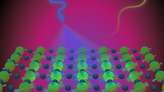
There are some ceramics that are excellent insulators at room temperature but that become perfect conductors when submersed in liquid nitrogen. However, this phenomenon, known as “high temperature” superconductivity, is not at all well understood by physicists. They theorize that at these temperatures, the collective quantum magnetic properties of the atoms in the material might come into play. But studying the magnetic properties of these materials at this minuscule scale would require years of effort.

Mark Dean, John Hill and Ivan Bozovic from Brookhaven National Laboratory (BNL), Thorsten Schmitt from Switzerland’s Paul Scherrer Institut (PSI), and Bastien Dalla Piazza and Henrik Ronnow from EPFL have unveiled the phenomena at work at this atomic scale. Using a unique device, the Brookhaven team created a layer just a single atom thick. Then, despite the material’s extreme thinness, the PSI scientists were able to use an ultrasensitive instrument to measure the magnetic dynamics of the atoms. And then EPFL provided the final piece of the puzzle, with mathematical models to analyze the measurements.

A long-awaited research tool


“We now have a kind of flashlight that will show us what direction we should take in our search,” explains Ronnow. Without understanding how these superconducting properties occurred at these temperatures, researchers were probing in the dark, using trial and error, to explore promising new materials. By combining these results with other recent work done by LQM researcher Nikolai Tsyrulin, the EPFL team has provided a new method to help physicists in their search for new superconductors. It’s a long-awaited step forward in the field; the Nobel Prize recognizing the discovery of high temperature superconductivity was awarded more than 25 years ago.

Promises for the future

Electrical resistance in traditional power lines leads to energy losses on the order of 3% in the electricity grid. At the scale of an entire country, this translates into several thousand gigawatts, which, in Switzerland’s case, would be the equivalent of the electricity consumption of a city the size of Geneva. “The energy challenges we face are significant; being able to use superconductivity won’t solve all of them, but it would nonetheless enable huge energy savings,” Ronnow adds.

Source: EPFL

Additional Information: 

Related Article:

Honda Develops New Technology to Weld Together Steel and Aluminum and Achieves World's First Application to the Frame of a Mass-production Vehicle

Engineerblogger
Sept. 9, 2012


Front Subframe


Honda Motor Company announced that it has newly developed a technology for the continuous welding of the dissimilar metals of steel and aluminum and applied it for the first time in the world to the subframe of a mass-production vehicle, a key component of a vehicle body frame. Honda will adopt this technology first to the North American version of the all-new 2013 Accord, which will go on sale in the United States on September 19, 2012, and will expand application sequentially to other models.


Conceptual diagram of FSW of dissimilar metals

Striving to reduce vehicle weight in order to increase fuel economy, Honda focused on Friction Stir Welding (FSW) and developed a new technology for the continuous welding of steel and aluminum. This technology generates a new and stable metallic bonding between steel and aluminum by moving a rotating tool on the top of the aluminum which is lapped over the steel with high pressure. As a result, the welding strength becomes equal to or beyond conventional Metal Inert Gas (MIG) welding*1.

This new technology contributes to an improvement in fuel economy by reducing body weight by 25% compared to a conventional steel subframe. In addition, electricity consumption during the welding process is reduced by approximately 50%. It also enabled a change in the structure of the subframe and the mounting point of suspension, which increased the rigidity of the mounting point by 20% and also contributed to the vehicle’s dynamic performance.

Furthermore, Honda established a new method to apply this technology to mass-production vehicles. Conventionally, FSW required use of large equipment, but Honda developed a FSW continuous welding system applied to a highly versatile industrial robot. This system also can be used for aluminum-to-aluminum welding and thus, the welding system with the same specifications can be used for production of a full-aluminum subframe.

Honda also developed a non-destructive inspection system*2 using a highly-sensitive infrared camera and laser beam, which enables an in-line inspection of the bonding location for every unit.

*1 A welding technique most commonly used for welding of identical materials such as steel-to-steel or aluminum-to-aluminum
*2A system that evaluates quality without actually destructing the parts


Source: Honda

Could ancient Egyptians hold the key to 3D printed ceramics?

Engineerblogger
Sept 3, 2012


Video: Professor Stephen Hoskins shares more about the latest 3D printing methods in ceramics in this insightful interview.
A 7,000 year old technique, known as Egyptian Paste (also known as Faience), could offer a potential process and material for use in the latest 3D printing techniques of ceramics, according to researchers at UWE Bristol.

Professor Stephen Hoskins, Director of UWE's Centre for Fine Print Research and David Huson, Research Fellow, have received funding from the Arts and Humanities Research Council (AHRC to undertake a major investigation into a self-glazing 3D printed ceramic, inspired by ancient Egyptian Faience ceramic techniques. The process they aim to develop would enable ceramic artists, designers and craftspeople to print 3D objects in a ceramic material which can be glazed and vitrified in one firing.

The researchers believe that it possible to create a contemporary 3D printable, once-fired, self-glazing, non-plastic ceramic material that exhibits the characteristics and quality of Egyptian Faience.

Faience was first used in the 5th Millennium BC and was the first glazed ceramic material invented by man. Faience was not made from clay (but instead composed of quartz and alkali fluxes) and is distinct from Italian Faience or Majolica, which is a tin, glazed earthenware. (The earliest Faience is invariably blue or green, exhibiting the full range of shades between them, and the colouring material was usually copper). It is the self-glazing properties of Faience that are of interest for this research project.

Current research in the field of 3D printing concentrates on creating functional materials to form physical models. The materials currently used in the 3D printing process, in which layers are added to build up a 3D form, are commonly: UV polymer resins, hot melted 'abs' plastic and inkjet binder or laser sintered, powder materials. These techniques have previously been known as rapid prototyping (RP). With the advent of better materials and equipment some RP of real materials is now possible. These processes are increasingly being referred to as solid 'free-form fabrication' (SFF) or additive layer manufacture. The UWE research team have focused previously on producing a functional, printable clay body.

This three-year research project will investigate three methods of glazing used by the ancient Egyptians: 'application glazing', similar to modern glazing methods; 'efflorescent glazing' which uses water-soluble salts; and 'cementation glazing', a technique where the object is buried in a glazing powder in a protective casing, then fired.These techniques will be used as a basis for developing contemporary printable alternatives

Professor Hoskins explains, “It is fascinating to think that some of these ancient processes, in fact the very first glazed ceramics every created by humans, could have relevance to the advanced printing technology of today. We hope to create a self-glazing 3D printed ceramic which only requires one firing from conception to completion rather than the usual two. This would be a radical step-forward in the development of 3D printing technologies. As part of the project we will undertake case studies of craft, design and fine art practitioners to contribute to the project, so that our work reflects the knowledge and understanding of artists and reflects the way in which artists work.”

The project includes funding for a three-year full-time PhD bursary to research a further method used by the Egyptians, investigating coloured 'frit', a substance used in glazing and enamels. This student will research this method, investigating the use of coloured frits and oxides to try and create as full a colour range as possible. Once developed, this body will be used to create a ceramic extrusion paste that can be printed with a low-cost 3D printer. A programme of work will be undertaken to determine the best rates of deposition, the inclusion of flocculants and methods of drying through heat whilst printing.

This project offers the theoretical possibility of a printed, single fired, glazed ceramic object - something that is impossible with current technology.

Source: University of the West of England

Manufacturing crack-resistant lightweight components

Enginerblogger
Sept 9, 2012


In this test, the material sample is heated to welding temperature to determine its critical conditions for the formation of cold cracking.  © Chair of Joining and Welding Technology at the Brandenburg University of Technology

Cars, roof structures and bridges should become increasingly lighter, with the same stability, and thus save energy and materials. New high-strength steel is superbly suited for the needed lightweight design, because it can also withstand extremely heavy stresses. Yet these materials also betray a disadvantage: with increasing strength their susceptibility to cold cracking rises when welded. These miniscule fractures might form as the welded joints cool off – typically at temperatures below 200°C. In a worst case scenario, the welding seams would crack. For this reason, many industrial sectors are reluctant to employ these promising high-strength steel.

Scientists at the Fraunhofer Institute for Mechanics of Materials IWM in Freiburg, in conjunction with the Chair of Joining and Welding Technology LFT at Brandenburg University of Technology Cottbus (BTU) developed a new process for making cold cracking more predictable. “We are able to compute the probability of cold cracking as early as the design stage of a component, and immediately run through corrective measures as well,” explains Frank Schweizer of the IWM. Because whether such cold cracking occurs, and how quickly, depends on how high the concentration of hydrogen in the steel is, how the residual stress turns out, and how its microstructure is configured. Predicting the probability of cracking has been difficult until now. Manufacturers used to conduct expensive testing, for example by applying an increasingly higher tensile stress to a sample component, and then analyse what stress level would cause cracking. Not only are these tests time-consuming and cost-intensive, the findings can-
not be applied to subsequent components on a one-to-one basis – because the geometry of the component has a decisive influence on crack formation. Even currently available computer simulations failed to deliver the desired predictive accuracy for real components.

Lowering production costs, shortening development phases

The new approach could markedly reduce such costly methods in the future – and thus lower production costs while shortening development phases. The experts at LFT set up a special test, in order to precisely determine the cracking criterion on samples of highstrength steel. Beside typical influencing factors like hydrogen content, residual stresses and material structures that can be adjusted in at the same time, they also take into account the temperature gradients that emerge in the welding process.

The experts at IWM feed a computer simulation with this criterion in order to analyze the threat of cold cracking in random components and geometries. “This way, we can locate the areas on a welding seam at risk of cold cracking, for each point and at any time in the simulated welding process,” explains Frank Schweizer. The researchers can also get a preliminary look at the effects of any countermeasures, and make the necessary adjustments. To do so, they transfert the results back into the simulation, in order to fine-tune them there.

In the future, with the aid of this process, manufacturers of vehicles and machines could be able to define non-critical welding parameters and limiting conditions for their materials in advance – and thus establish a substantially more efficient and safer production process. This is especially relevant to materials that are difficult to weld, with very narrow processing windows regarding welding parameters or the pre- and post-heating temperatures. Fraunhofer IWM and LFT, in cooperation with Robert Bosch GmbH and ThyssenKrupp Steel Europe AG, are currently testing their new process on laser beam-welded demonstration models made of high-strength steels.

Boaz Almog “levitates” a superconductor

Engineerblogger
Sept 9, 2012


How can a super-thin 3-inch disk levitate something 70,000 times its own weight? In a riveting demonstration, Boaz Almog shows how a phenomenon known as quantum locking allows a superconductor disk to float over a magnetic rail -- completely frictionlessly and with zero energy loss.

Experiment: Prof. Guy Deutscher, Mishael Azoulay, Boaz Almog, of the High Tc Superconductivity Group, School of Physics and Astronomy, Tel Aviv University.

Source: TED

Saturday 8 September 2012

Researchers create tiny, wirelessly powered cardiac device

Engineerblogger
Sept 9, 2012

Ada Poon, assistant professor of electrical engineering, led the research. (Photo: Linda A. Cicero / Stanford News Service)

Stanford electrical engineers overturn existing models to demonstrate the feasibility of a millimeter-sized, wirelessly powered cardiac device. The findings, say the researchers, could dramatically alter the scale of medical devices implanted in the human body.

A team of engineers at Stanford has demonstrated the feasibility of a super-small, implantable cardiac device that gets its power not from batteries but from radio waves transmitted from a small power device on the surface of the body.

The implanted device is contained in a cube just 0.8 millimeter on a side. It could fit on the head of pin.

The findings were published in the journal Applied Physics Letters. In their paper, the researchers demonstrated wireless power transfer to a millimeter-sized device implanted 5 centimeters inside the chest on the surface of the heart – a depth once thought out of reach for wireless power transmission.

The engineers say the research is a major step toward a day when all implants are driven wirelessly. Beyond the heart, they believe such devices might include swallowable endoscopes – so-called "pillcams" that travel the digestive tract – permanent pacemakers and precision brain stimulators – virtually any medical applications where device size and power matter.
A revolution in the body

Implantable medical devices in the human body have revolutionized medicine. Hundreds of thousands if not millions of pacemakers, cochlear implants and drug pumps are today helping patients live relatively normal lives, but these devices are not without engineering challenges.

First, they require power, which means batteries, and batteries are bulky. In a device like a pacemaker, the battery alone accounts for as much as half the volume of the device. Second, batteries have finite lives. New surgery is needed when they wane.

"Wireless power solves both challenges," said Ada Poon, assistant professor of electrical engineering, who headed up the research. She was assisted by Sanghoek Kim and John Ho, both doctoral candidates in her lab.

Last year, Poon made headlines when she demonstrated a wirelessly powered, self-propelled device capable of swimming through the bloodstream. To get there she needed to overturn some long-held assumptions about delivery of wireless power through the human body.

Her latest device works by a combination of inductive and radiative transmission of power. Both are types of electromagnetic transfer in which a transmitter sends radio waves to a coil of wire inside the body. The radio waves produce an electrical current in the coil sufficient to operate a small device.

There is an indirect relationship between the frequency of the transmitted radio waves and the size of the receiving antenna. That is, to deliver a desired level of power, lower frequency waves require bigger coils. Higher frequency waves can work with smaller coils.

"For implantable medical devices, therefore, the goal is a high-frequency transmitter and a small receiver, but there is one big hurdle," Kim said.
Ignoring consensus

Existing mathematical models have held that high-frequency radio waves do not penetrate far enough into human tissue, necessitating the use of low-frequency transmitters and large antennas – too large to be practical for implantable devices.

Ignoring the consensus, Poon proved the models wrong. Human tissues dissipate electric fields quickly, it is true, but radio waves can travel in a different way – as alternating waves of electric and magnetic fields. With the correct equations in hand, she discovered that high-frequency signals travel much deeper than anyone suspected.

"In fact, to achieve greater power efficiency, it is actually advantageous that human tissue is a very poor electrical conductor," said Kim. "If it were a good conductor, it would absorb energy, create heating and prevent sufficient power from reaching the implant."

According to their revised models, the researchers found that the maximum power transfer through human tissue occurs at about 1.7 billion cycles per second, much higher than previously thought.

"In this high-frequency range, we can increase power transfer by about 10 times over earlier devices," said Ho, who honed the mathematical models.

The discovery meant that the team could shrink the receiving antenna by a factor of 10 as well, to a scale that makes wireless implantable devices feasible. At the optimal frequency, a millimeter-radius coil is capable of harvesting more than 50 microwatts of power, well in excess of the needs of a recently demonstrated 8-microwatt pacemaker.
Engineering challenges

With the dimensional challenges solved, the team found itself bound by other engineering constraints. First, electronic medical devices must meet stringent health standards established by IEEE (Institute of Electrical and Electronics Engineers), particularly with regard to tissue heating. Second, the team found that the receiving and transmitting antennas had to be optimally oriented to achieve maximum efficiency. Differences in alignment of just a few degrees could produce troubling drops in power.

"This can't happen medical devices," said Poon. "As the human heart and body are in constant motion, solving this issue was critical to the success of our research." The team responded by designing an innovative slotted transmitting antenna structure. It delivers consistent power efficiency regardless of orientation of the two antennas.

The new design serves additionally to focus the radio waves precisely at the point inside the body where the implanted device rests on the surface of the heart – increasing the electric field where it is needed most, but canceling it elsewhere. This helps reduce overall tissue heating to levels well within the IEEE standards. Poon has applied for a patent on the antenna structure.

This research was made possible by funding from the C2S2 Focus Center, one of six research centers funded under the Focus Center Research Program, a Semiconductor Research Corporation entity. Lisa Chen also contributed to this study.

Source: Stanford University

Researchers Develop New, Less Expensive Nanolithography Technique

Engineerblogger
Sept 9, 2012


This technique uses no electronic components to bring the cantilevers into contact with the substrate surface.

Researchers from North Carolina State University have developed a new nanolithography technique that is less expensive than other approaches and can be used to create technologies with biomedical applications.

“Among other things, this type of lithography can be used to manufacture chips for use in biological sensors that can identify target molecules, such as proteins or genetic material associated with specific medical conditions,” says Dr. Albena Ivanisevic, co-author of a paper describing the research. Ivanisevic is an associate professor of materials science and engineering at NC State and associate professor of the joint biomedical engineering program at NC State and the University of North Carolina at Chapel Hill. Nanolithography is a way of printing patterns at the nanoscale.

The new technique relies on cantilevers, which are 150-micron long silicon strips. The cantilevers can be tipped with spheres made of polymer or with naturally occurring spores. The spheres and spores are coated with ink and dried. The spheres and spores are absorbent and will soak up water when exposed to increased humidity.

As a result, when the cantilevers are exposed to humidity in a chamber, the spheres and spores absorb water – making the tips of the cantilevers heavier and dragging them down into contact with any chosen surface.

Users can manipulate the size of the spheres and spores, which allows them to control the patterns created by the cantilevers. For example, at low humidity, a large sphere will absorb more water than a small sphere, and will therefore be dragged down into contact with the substrate surface. The small sphere won’t be lowered into contact with the surface until it is exposed to higher humidity and absorbs more water.

Further, the differing characteristics of sphere polymers and spores mean that they absorb different amounts of water when exposed to the same humidity – giving users even more control of the nanolithography.

“This technique is less expensive than other device-driven lithography techniques used for microfabrication because the cantilevers do not rely on electronic components to bring the cantilevers into contact with the substrate surface,” Ivanisevic says. “Next steps for this work include using this approach to fabricate lithographic patterns onto tissue for use in tissue regeneration efforts.”

The paper, “Parallel Dip-Pen Nanolithography using Spore- and Colloid-Terminated Cantilevers,” was published online Aug. 17 in the journal Small. Lead author of the paper is Dr. Marcus A. Kramer, who did the work at NC State while completing his Ph.D. at Purdue University.


Source: North Carolina State University

Reference Material Could Aid Nanomaterial Toxicity Research

Engineerblogger
Sept 9, 2012


TEM image shows the nanoscale crystalline structure of titanium dioxide in NIST SRM 1898 (color added for clarity.)  Credit: Impellitteri/EPA
The National Institute of Standards and Technology (NIST) has issued a new nanoscale reference material for use in a wide range of environmental, health and safety studies of industrial nanomaterials. The new NIST reference material is a sample of commercial titanium dioxide powder commonly known as “P25.”

NIST Standard Reference Materials® (SRMs) are typically samples of industrially or clinically important materials that have been carefully analyzed by NIST. They are provided with certified values for certain key properties so that they can be used in experiments as a known reference point.

Nanoscale titanium-dioxide powder may well be the most widely manufactured and used nanomaterial in the world, and not coincidentally, it is also one of the most widely studied. In the form of larger particles, titanium dioxide is a common white pigment. As nanoscale particles, the material is widely used as a photocatalyst, a sterilizing agent and an ultraviolet blocker (in sunscreen lotions, for example).

“Titanium dioxide is not considered highly toxic and, in fact, we don’t certify its toxicity,” observes NIST chemist Vincent Hackley. “But it’s a representative industrial nanopowder that you could include in an environmental or toxicity study. It’s important in such research to include measurements that characterize the nanomaterial you’re studying—properties like morphology, surface area and elemental composition. We’re providing a known benchmark.”

The new titanium-dioxide reference material is a mixed phase, nanocrystalline form of the chemical in a dry powder. To assist in its proper use, NIST also has developed protocols* for properly preparing samples for environmental or toxicological studies.

The new SRM also is particularly well suited for use in calibrating and testing analytical instruments that measure specific surface area of nanomaterials by the widely used Brunauer-Emmet-Teller (BET) gas sorption method.

Additional details and purchasing information on NIST Standard Reference Material 1898, “Titanium Dioxide Nanomaterial” are available at www.nist.gov/srm/index.cfm.

SRMs are among the most widely distributed and used products from NIST. The agency prepares, analyzes and distributes nearly 1,300 different materials that are used throughout the world to check the accuracy of instruments and test procedures used in manufacturing, clinical chemistry, environmental monitoring, electronics, criminal forensics and dozens of other fields.


Source: The National Institute of Standards and Technology (NIST)

Additional Information:

Researchers Set World Record for Highest Surface Area Material

Engineerblogger
Sept 9, 2012


Northwestern University researchers have broken a world record by creating two new synthetic materials with the greatest amount of surface areas reported to date.

Named NU-109 and NU-110, the materials belong to a class of crystalline nanostructure known as metal-organic frameworks (MOFs) that are promising vessels for natural gas storage for vehicles, catalysts, and other sustainable materials chemistry.

The materials’ promise lies in their vast internal surface area. If the internal surface area of one NU-110 crystal the size of a grain of salt could be unfolded, the surface area would cover a desktop. Put another way, the internal surface area of one gram of NU-110 would cover one-and-a-half football fields.

A paper describing the findings, “Metal-organic Framework Materials with Ultrahigh Surface Areas: Is the Sky the Limit?” was published August 20 in the Journal of the American Chemical Society.

The research team, led by Omar Farha, research associate professor of chemistry in the Weinberg College of Arts and Sciences, has synthesized, characterized, and computationally simulated the behavior of the two MOFs that display the highest experimental Brunauer-Emmett-Teller surface areas of any porous material on record, 7,000 m2/g; that is, one kilogram of the material contains an internal surface area that could cover seven square kilometers. (Brunauer-Emmett-Teller, or BET, is an analysis technique for measuring the surface area of a material.)

The extremely high surface area, which is normally not accessible due to solvent molecules that stay trapped within the pores, was achieved using a carbon dioxide activation technique. As opposed to heating, which can remove the solvent but also damage the MOF material, the carbon dioxide-based technique removes the solvent gently and leaves the pores completely intact.

The development could rapidly lead to further advances. MOFs are composed of organic linkers held together by metal atoms, resulting in a molecular cage-like structure. The researchers believe they may be able to more than double the surface area of the materials by using less bulky linker units in the materials’ design.

The research comes from the labs of Joseph T. Hupp, professor of chemistry in Weinberg, and Randall Q. Snurr, professor of chemical and biological engineering at the McCormick School of Engineering.

Other authors include SonBinh Nguyen, professor of chemistry in Weinberg; Ibrahim Eryazici, Nak Cheon Jeong, Brad G. Hauser, Amy A. Sarjeant, and Christopher E. Wilmer, all of Northwestern; and A. Özgür Yazaydın of the University of Surrey in the United Kingdom.

The MOF-designing and -synthesizing technology is being commercialized by NuMat Technologies, a Northwestern startup that has won more than $1 million in business plan competitions since incorporating in February.

Source:  Northwestern University