Feb 3, 2012
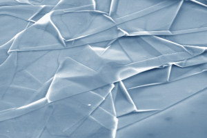 |
| Graphene nanofabric. SEM micrograph of a strongly crumpled graphene sheet on a Si wafer. Note that it looks just like silk thrown over a surface. Lateral size of the image is 20 microns. Si wafer is at the bottom-right corner. Credit: University of Manchester |
In a paper published this week in Science, a Manchester team lead by Nobel laureates Professor Andre Geim and Professor Konstantin Novoselov has literally opened a third dimension in graphene research. Their research shows a transistor that may prove the missing link for graphene to become the next silicon.
Graphene – one atomic plane of carbon – is a remarkable material with endless unique properties, from electronic to chemical and from optical to mechanical.
One of many potential applications of graphene is its use as the basic material for computer chips instead of silicon. This potential has alerted the attention of major chip manufactures, including IBM, Samsung, Texas Instruments and Intel. Individual transistors with very high frequencies (up to 300 GHz) have already been demonstrated by several groups worldwide.
Unfortunately, those transistors cannot be packed densely in a computer chip because they leak too much current, even in the most insulating state of graphene. This electric current would cause chips to melt within a fraction of a second.
This problem has been around since 2004 when the Manchester researchers reported their Nobel-winning graphene findings and, despite a huge worldwide effort to solve it since then, no real solution has so far been offered.
The University of Manchester scientists now suggest using graphene not laterally (in plane) – as all the previous studies did – but in the vertical direction. They used graphene as an electrode from which electrons tunnelled through a dielectric into another metal. This is called a tunnelling diode.
Then they exploited a truly unique feature of graphene – that an external voltage can strongly change the energy of tunnelling electrons. As a result they got a new type of a device – vertical field-effect tunnelling transistor in which graphene is a critical ingredient.
Dr Leonid Ponomarenko, who spearheaded the experimental effort, said: “We have proved a conceptually new approach to graphene electronics. Our transistors already work pretty well. I believe they can be improved much further, scaled down to nanometre sizes and work at sub-THz frequencies.”
“It is a new vista for graphene research and chances for graphene-based electronics never looked better than they are now”, adds Professor Novoselov.
Graphene alone would not be enough to make the breakthrough. Fortunately, there are many other materials, which are only one atom or one molecule thick, and they were used for help.
The Manchester team made the transistors by combining graphene together with atomic planes of boron nitride and molybdenum disulfide. The transistors were assembled layer by layer in a desired sequence, like a layer cake but on an atomic scale.
Such layer-cake superstructures do not exist in nature. It is an entirely new concept introduced in the report by the Manchester researchers. The atomic-scale assembly offers many new degrees of functionality, without some of which the tunnelling transistor would be impossible.
“The demonstrated transistor is important but the concept of atomic layer assembly is probably even more important,” explains Professor Geim.
Professor Novoselov added: “Tunnelling transistor is just one example of the inexhaustible collection of layered structures and novel devices which can now be created by such assembly.
“It really offers endless opportunities both for fundamental physics and for applications. Other possible examples include light emission diodes, photovoltaic devices, and so on.”
Source: University of Manchester
Additional Information:
- The abstract of "Field-effect tunneling transistor based on vertical graphene heterostructures", by L. Britnel1, R. Gorbache2, R. Jalil, B. Bell2, F. Schedin, A. Mishchenko, T. Georgiou, M. Katsnelson, L. Eaves, S. Morozov, N. Peres, J. Leist, A. Geim, K. Novoselov, and L. Ponomarenko in Science Journal.
0 comments:
Post a Comment