Blogger Themes

Saturday, 5 January 2013

Jumping droplets help heat transfer

Engineerblogger
Jan 4, 2013


Many industrial plants depend on water vapor condensing on metal plates: In power plants, the resulting water is then returned to a boiler to be vaporized again; in desalination plants, it yields a supply of clean water. The efficiency of such plants depends crucially on how easily droplets of water can form on these metal plates, or condensers, and how easily they fall away, leaving room for more droplets to form.

The key to improving the efficiency of such plants is to increase the condensers’ heat-transfer coefficient — a measure of how readily heat can be transferred away from those surfaces, explains Nenad Miljkovic, a doctoral student in mechanical engineering at MIT. As part of his thesis research, he and colleagues have done just that: designing, making and testing a coated surface with nanostructured patterns that greatly increase the heat-transfer coefficient.

The results of that work have been published in the journal Nano Letters, in a paper co-authored by Miljkovic, mechanical engineering associate professor Evelyn Wang, and five other researchers from the Device Research Lab (DRL) in MIT’s mechanical engineering department.

On a typical, flat-plate condenser, water vapor condenses to form a liquid film on the surface, drastically reducing the condenser’s ability to collect more water until gravity drains the film. “It acts as a barrier to heat transfer,” Miljkovic says. He and other researchers have focused on ways of encouraging water to bead up into droplets that then fall away from the surface, allowing more rapid water removal.

“The way to remove the thermal barrier is to remove [the droplets] as quickly as possible,” he says. Many researchers have studied ways of doing this by creating hydrophobic surfaces, either through chemical treatment or through surface patterning. But Miljkovic and his colleagues have now taken this a step further by making scalable surfaces with nanoscale features that barely touch the droplets.

The result: Droplets don’t just fall from the surface, but actually jump away from it, increasing the efficiency of the process. The energy released as tiny droplets merge to form larger ones is enough to propel the droplets upward from the surface, meaning the removal of droplets doesn’t depend solely on gravity.


Jumping-droplet superhydrophobic condensation shown on a nanostructured CuO tube.
Image courtesy of the researchers


 Other researchers have worked on nanopatterned surfaces to induce such jumping, but these have tended to be complex and expensive to manufacture, usually requiring a clean-room environment. Those approaches also require flat surfaces, not the tubing or other shapes often used in condensers. Finally, prior research has not tested the enhanced heat transfer predicted for these types of surfaces.

In a paper published early in 2012, the MIT researchers showed that droplet shape is important to enhanced heat transfer. “Now, we’ve gone a step further,” Miljkovic says, “developing a surface that favors these kinds of droplets, while being highly scalable and easy to manufacture. Furthermore, we’ve actually been able to experimentally measure the heat-transfer enhancement.”

The patterning is done, Miljkovic says, using a simple wet-oxidation process right on the surface that can be applied to the copper tubes and plates commonly used in commercial power plants.

The nanostructured pattern itself is made of copper oxide and actually forms on top of the copper tubing. The process produces a surface that resembles a bed of tiny, pointed leaves sticking up from the surface; these nanoscale points minimize contact between the droplets and the surface, making release easier.

Not only can the nanostructured patterns be made and applied under room-temperature conditions, but the growth process naturally stops itself. “It’s a self-limiting reaction,” Miljkovic says, “whether you put it in [the treatment solution] for two minutes or two hours.”

After the leaflike pattern is created, a hydrophobic coating is applied when a vapor solution bonds itself to the patterned surface without significantly altering its shape. The team’s experiments showed that the efficiency of heat transfer using these treated surfaces could be increased by 30 percent, compared to today’s best hydrophobic condensing surfaces.

That means, Miljkovic says, that the process lends itself to retrofitting thousands of power plants already in operation around the world. The technology could also be useful for other processes where heat transfer is important, such as in dehumidifiers and for heating and cooling systems for buildings, the authors say.

Challenges for this approach remain, Miljkovic says: If too many droplets form, they can “flood” the surface, reducing its heat-transfer ability. “We are working on delaying this surface flooding and creating more robust solutions that can work well [under] all operating conditions,” he says.

Yi Cui, an associate professor of materials science and engineering at Stanford University, calls the concept behind this work “an excellent idea,” and adds, “The studies here can lead to better atmospheric water-harvesting and dehumidification, and efficient heat transfer.” Cui adds that the fact that this team was able to make direct measurements of the actual heat-transfer enhancement from these treated surfaces is “interesting and important.”

The research team also included postdocs Ryan Enright and Youngsuk Nam and undergraduates Ken Lopez, Nicholas Dou and Jean Sack, all of MIT’s mechanical engineering department. The work was supported by MIT’s Solid-State Solar Thermal Energy Conversion Center, the U.S. Department of Energy, the National Science Foundation and the Irish Research Council for Science, Engineering and Technology.

Source: MIT

New 2D material for next generation high-speed electronics

Engineerblogger
Jan 4, 2013

Artist impression of high carrier mobility through layered molybdenum oxide crystal lattice. Credit: Dr Daniel J White, ScienceFX

Scientists at CSIRO and RMIT University have produced a new two-dimensional material that could revolutionise the electronics market, making “nano” more than just a marketing term.

The material – made up of layers of crystal known as molybdenum oxides – has unique properties that encourage the free flow of electrons at ultra-high speeds.

In a paper published in the January issue of materials science journal Advanced Materials, the researchers explain how they adapted a revolutionary material known as graphene to create a new conductive nano-material.

Graphene was created in 2004 by scientists in the UK and won its inventors a Nobel Prize in 2010. While graphene supports high speed electrons, its physical properties prevent it from being used for high-speed electronics.

The CSIRO's Dr Serge Zhuiykov said the new nano-material was made up of layered sheets – similar to graphite layers that make up a pencil's core.

"Within these layers, electrons are able to zip through at high speeds with minimal scattering," Dr Zhuiykov said.

"The importance of our breakthrough is how quickly and fluently electrons – which conduct electricity – are able to flow through the new material."

RMIT's Professor Kourosh Kalantar-zadeh said the researchers were able to remove "road blocks" that could obstruct the electrons, an essential step for the development of high-speed electronics.

"Instead of scattering when they hit road blocks, as they would in conventional materials, they can simply pass through this new material and get through the structure faster," Professor Kalantar-zadeh said.

"Quite simply, if electrons can pass through a structure quicker, we can build devices that are smaller and transfer data at much higher speeds.

"While more work needs to be done before we can develop actual gadgets using this new 2D nano-material, this breakthrough lays the foundation for a new electronics revolution and we look forward to exploring its potential."

In the paper titled 'Enhanced Charge Carrier Mobility in Two-Dimensional High Dielectric Molybdenum Oxide,' the researchers describe how they used a process known as "exfoliation" to create layers of the material ~11nm thick.

The material was manipulated to convert it into a semiconductor and nanoscale transistors were then created using molybdenum oxide.

The result was electron mobility values of  >1,100 cm2/Vs – exceeding the current industry standard for low dimensional silicon.

The work, with RMIT doctoral researcher Sivacarendran Balendhran as the lead author, was supported by the CSIRO Sensors and Sensor Networks Transformational Capability Platform and the CSIRO Materials Science and Engineering Division.

It was also a result of collaboration between researchers from Monash University, University of California – Los Angeles (UCLA), CSIRO, Massachusetts Institute of Technology (MIT) and RMIT.

Source:  CSIRO

Doris Kim Sung: Metal that breathes

Engineerblogger
Jan 4, 2013

Modern buildings with floor-to-ceiling windows give spectacular views, but they require a lot of energy to cool. Doris Kim Sung works with thermo-bimetals, smart materials that act more like human skin, dynamically and responsively, and can shade a room from sun and self-ventilate.

Doris Kim Sung is a biology student turned architect interested in thermo-bimetals, smart materials that respond dynamically to temperature change.


Source:  Ted

Additional Information:

Sunday, 28 October 2012

Targeted dissolution: the new generation of implants

Engineerblogger
Oct 27, 2012


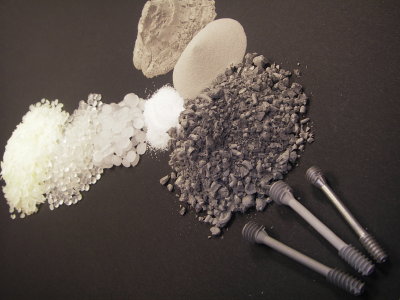
Metal powder injection molding: Top right the metal powders and polymer components left, center: the mixed Granualt. Below: component precursors, and the final Mg-Ca-bone screw to the right. [Photo:HZG/M. Wolff]


Is a paradigm shift imminent in the field of implant materials? Scientists at the Helmholtz Zentrum Geesthacht are engaged in research on biodegradable magnesium biomaterials which can be used as bone replacements in medical applications. They will present their research results from the 1st to 3rd November at the annual congress of the DGBM (German society for Biomaterials) in Hamburg.


When autumn arrives it brings wind and rain, leaves fall from the trees and settle on the ground. If someone slips on them, a bone can easily be broken. When a nail or a plate is required for the fixation of such a bone fracture, it is nowadays usually made of titanium, as this material is stable and well-tolerated by the human body. However, this foreign body must often be removed after the bone has healed, as there is otherwise a danger of inflammation or even bone loss.

According to Prof. Dr. Regine Willumeit, the head of the ‘Structural Research on Macromolecules’ department at the Helmholtz-Zentrum Geesthacht: “The aim of modern implant research is to develop a material which can be used in the body like a real replacement material. A biomaterial which at first supports the bone but then disappears of its own accord after the bone has recovered”.

Magnesium is excellently suited to this purpose. This element is naturally present in the human body and has the advantage that it can biodegrade in a pre-determined manner. It must, thereby, be both light and strong but also well-tolerated by the body. Research scientists at the Helmholtz-Zentrum in Geesthacht are therefore focussing their attention on this particular biomaterial.

The Helmholtz-Zentrum in Geesthacht has shown great expertise for many years in the research and production of prototypes for metallic biodegradable magnesium alloy implants. Material researchers are, for example, engaged in investigations into innovative magnesium-calcium alloys. These reveal material properties similar to those in bone; they are firm and at the same time elastic. Calcium appears to be well suited as an alloy as it would be able to degrade into non-toxic products in the body in the same way as magnesium. The degradation products would even be able to stimulate bone growth.

As Prof. Dr. Regine Willumeit explains: “ We are developing alloys in Geesthacht which have extremely promising properties for use in orthopaedic and traumatological applications. The colleagues at the Magnesium Innovations Center, MagIC, at the HZG, provide us with the starting material, we examine the factors which determine the degradation of the magnesium under physiological conditions”.

Scientists are not only engaged in research into the degradation process of the material itself. Tests are carried out in the Geesthacht laboratories in cell culture on the effects of the degradation on surrounding cells, for example. The scientists involved in this fundamental research into innovative implant materials have comprehensive analysis and test methods at their disposal.

As stable as bone, yet with good biodegradability


Would spare the second operation for removal of screws and plates: implant material of biodegradable magnesium [Photo: Istock 21545233]

The development of production processes is still causing researchers headaches. However, they have also made great progress in this area. The scientist Martin Wolff, from the powder technology department, has, for the first time, succeeded in producing magnesium-calcium bone screws by means of the metal powder injection molding process (MIM). 

As he explains: “The challenge in the case of magnesium lies in the high affinity of this material for oxygen. However, even small amounts of oxygen lead to dramatic changes in the mechanical properties of the component. Calcium, as an alloy partner, captures the oxygen in the production process during the so-called sintering procedure, and the material thus becomes firmer. This non-toxic alloying element has proved successful in achieving better results, at least in experiments. However, numerous further investigations now lie ahead, e.g. in cell culture and in the organism, before this material can be utilized as an implant material.

The Helmholtz researchers from Geesthacht will present their results at the Annual Congress of the Deutsche Gesellschaft für Biomaterialien, DGBM (German Society for Biomaterials), which is to be held at the Chamber of Commerce in Hamburg from 1st to 3rd of November 2012. The main focus this year will be on “Degradable Implants and Biomaterials”. The Congress will be led by Prof. Dr. Regine Willumeit.

Source:  Helmholtz Zentrum Geesthacht


Additional Information:
 
  • Poster Rapid Fire Presentation

New format for the presentation of research results. The scientist’s own research field and results must be clearly presented in only five minutes.
  • Metal powder injection moulding MIM

MIM uses injection moulding technology for the shaping process, which is also widely used in the field of plastics. The starting material is a fine metal powder which is mixed with a so-called binder. This mixture is fused at approx. 100 degrees centigrade. The binder is then chemically removed from the injection moulded part so that only the metal remains. The powder is compacted to the desired firm and dense body by means of a sintering process. 


Friday, 26 October 2012

Reclaiming rare earths: Laboratory improving process to recycle rare-earth materials

Engineerblogger
Oct 26, 2012
 
Rare-earth magnet scraps are melted in a furnace with magnesium.
Scientists at the Ames Laboratory are improving the process to reclaim
rare-earth materials.

Recycling keeps paper, plastics, and even jeans out of landfills. Could recycling rare-earth magnets do the same? Perhaps, if the recycling process can be improved.

Scientists at the U.S. Department of Energy’s (DOE) Ames Laboratory are working to more effectively remove the neodymium, a rare earth element, from the mix of other materials in a magnet. Initial results show recycled materials maintain the properties that make rare-earth magnets useful.

The current rare earth recycling research builds on Ames Laboratory’s decades of rare-earth processing experience. In the 1990s, Ames Lab scientists developed a process that uses molten magnesium to remove rare earths from neodymium-iron-boron magnet scrap. Back then, the goal was to produce a mixture of magnesium and neodymium because the neodymium added important strength to the alloy, rather than separate out high-purity rare earths because, at the time, rare earth prices were low.

But rare earth prices increased ten-fold between 2009 and 2011 and supplies are in question. Therefore, the goal of today’s rare-earth recycling research takes the process one step farther.

“Now the goal is to make new magnet alloys from recycled rare earths. And we want those new alloys to be similar to alloys made from unprocessed rare-earth materials,” said Ryan Ott, the Ames Laboratory scientist leading the research. “It appears that the processing technique works well. It effectively removes rare earths from commercial magnets.”

Ott’s research team also includes Ames Laboratory scientist Larry Jones and is funded through a work for others agreement with the Korea Institute of Industrial Technology. The research group is developing and testing the technique in Ames Lab’s Materials Preparation Center, with a suite of materials science tools supported by the DOE Office of Science.

“We start with sintered, uncoated magnets that contain three rare earths: neodymium, praseodymium and dysprosium,” said Ott. “Then we break up the magnets in an automated mortar and pestle until the pieces are 2-4 millimeters long.

Next, the tiny magnet pieces go into a mesh screen box, which is placed in a stainless-steel crucible. Technicians then add chunks of solid magnesium.

A radio frequency furnace heats the material. The magnesium begins to melt, while the magnet chunks remain solid.

“What happens then is that all three rare earths leave the magnetic material by diffusion and enter the molten magnesium,” said Ott. “The iron and boron that made up the original magnet are left behind.”

The molten magnesium and rare-earth mixture is cast into an ingot and cooled. Then they boil off the magnesium, leaving just the rare earth materials behind.

“We’ve found that the properties of the recycled rare earths compare very favorably to ones from unprocessed materials,” said Ott. “We’re continuing to identify the ideal processing conditions.”

The next step is optimizing the extraction process. Then the team plans to demonstrate it on a larger scale.

“We want to help bridge the gap between the fundamental science and using this science in manufacturing,” said Ott. “And Ames Lab can process big enough amounts of material to show that our rare-earth recycling process works on a large scale.”

Source: Ames Laboratory

Electron 'sniper' targets graphene

Engineerblogger
Oct 26, 2012


Credit: Oxford University

Because of its intriguing properties graphene could be the ideal material for building new kinds of electronic devices such as sensors, screens, or even quantum computers.

One of the keys to exploiting graphene's potential is being able to create atomic-scale defects – where carbon atoms in its flat, honeycomb-like structure are rearranged or 'knocked out' – as these influence its electrical, chemical, magnetic, and mechanical properties.

A team led by Oxford University scientists report in Nature Communications a new approach to a new approach to engineering graphene's atomic structure with unprecedented precision.

'Current approaches for producing defects in graphene are either like a 'shotgun' where the entire sample is sprayed with high energy ions or electrons to cause widespread defects, or a chemistry approach where many regions of the graphene are chemically reacted,' said Jamie Warner from Oxford University's Department of Materials, a member of the team.

'Both methods lack any form of control in terms of spatial precision and also the defect type, but to date are the only reported methods known for defect creation.'

The new method replaces the 'shotgun' with something more like a sniper rifle: a minutely-controlled beam of electrons fired from an electron microscope.

'The shotgun approach is restricted to micron scale precision, which is roughly an area of 10,000,000 square nanometres, we demonstrated a precision to within 100 square nanometres, which is about four orders of magnitude better,' explains Alex Robertson of Oxford University's Department of Materials, another member of the team.

Yet it isn’t just about the accuracy of a single 'shot'; the researchers also show that by controlling the length of time graphene is exposed to their focused beam of electrons they can control the size and type of defect created.

'Our study reveals for the first time that only a few types of defects are actually stable in graphene, with several defects being quenched by surface atoms or relaxing back to pristine by bond rotations,' Jamie tells me.

The ability to create just the right kind of stable defects in graphene's crystal structure is going to be vital if its properties are to be harnessed for applications such as mobile phones and flexible displays.

'Defect sites in graphene are much more chemically reactive, so we can use defects as a site for chemical functionalisation of the graphene. So we can attach certain molecules, such as biomolecules, to the graphene to act as a sensor,' Alex tells me.

'Defects in graphene can also give rise to localized electron spin, an attribute that has important future use in quantum nanotechnology and quantum computers.'

At the moment scaling up the team's technique into a manufacturing process to create graphene-based technologies is still a way off. Currently electron microscopes are the only systems that can achieve the necessary exquisite control of an electron beam.

But, Alex says, it is always possible that a scalable electron beam lithography type technique may be developed in the future that could allow for defect patterning in graphene.And it's worth remembering that it wasn't so long ago that the technology needed to etch millions of transistors onto a tiny slice of silicon seemed like an impossible dream.

Source: Oxford University

Additional Information:

Abu Dhabi Scientists Create Desert Rainstorms: Report

Engineerblogger
Oct 26, 2012
Credit: AP

Desert dwellers wishing to transform their arid surroundings into a profitable, crop-sustaining oasis have reportedly gotten one step closer to making that dream a reality, as Abu Dhabi scientists now claim to have created more than 50 artificial rainstorms from clear skies during peak summer months in 2010.

According to Arabian Business, the storms were part of a top secret, Swiss-backed project, commissioned by Sheikh Khalifa bin Zayed Al Nahyan, president of the UAE and leader of Abu Dhabi. Called "Weathertec," the climate project -- said to be worth a staggering $11 million -- utilized ionizers resembling giant lampshades to generate fields of negatively charged particles, which create cloud formation, throughout the country's Al Ain region, the Telegraph is reporting.

"We are currently operating our innovative rainfall enhancement technology, Weathertec, in the region of Al Ain in Abu Dhabid," Helmut Fluhrer, the founder of Metro Systems International, the Swiss company in charge of the project, is quoted as saying. "We started in June 2010 and have achieved a number of rainfalls."

Monitored by the Max Planck Institute for Technology, a leading tank for the study of atmosphere physics, the fake storms are said to have baffled Abu Dhabi residents by also producing hail, wind gales and even lightning.

"There are many applications," Professor Hartmut Grassl, a former institute director, is quoted by the Daily Mail as saying. "One is getting water into a dry area. Maybe this is a most important point for mankind."

Source: Huffington Post

Related Information: